Copper plating layer voids on circuit board hole walls
 Jun. 21, 2023
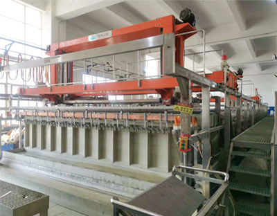
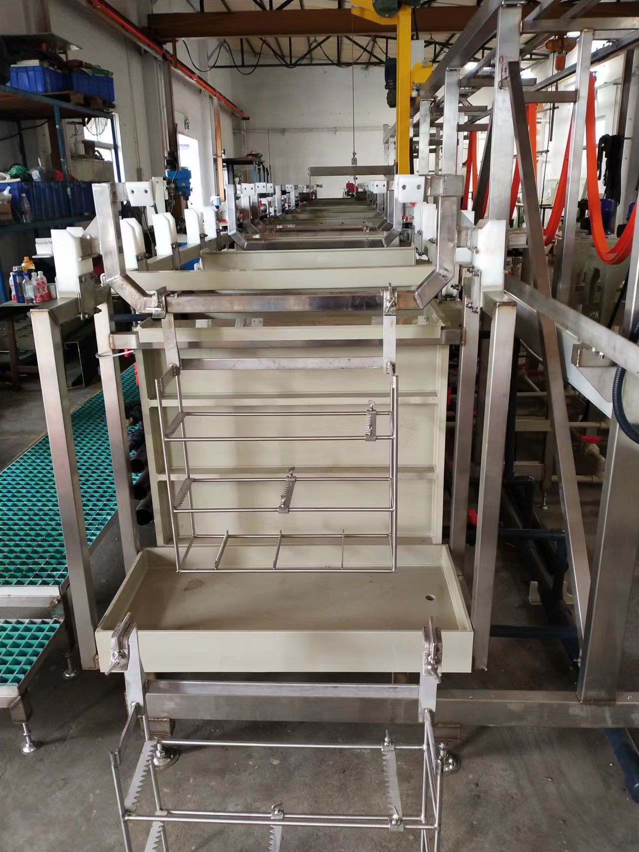
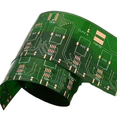
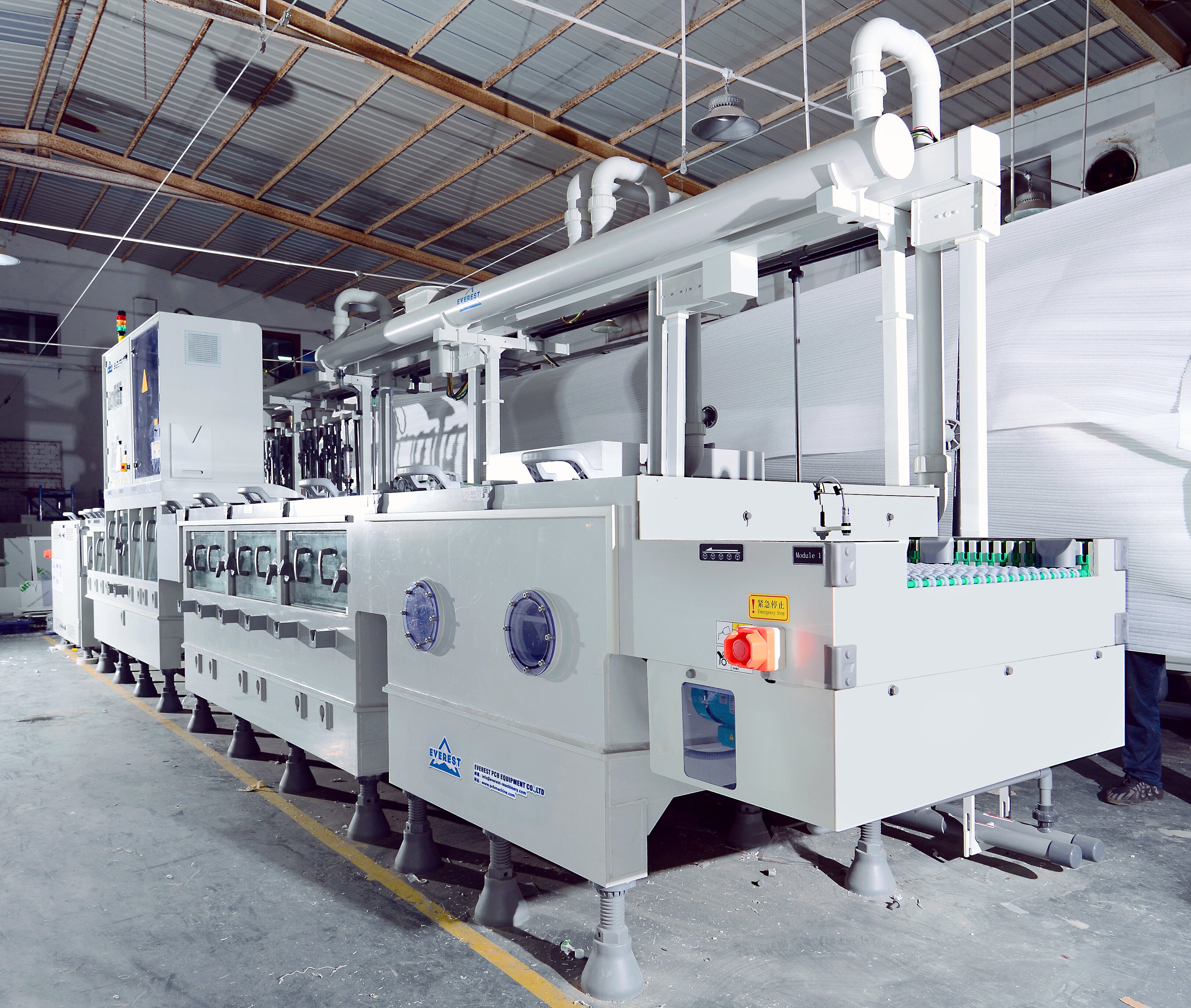
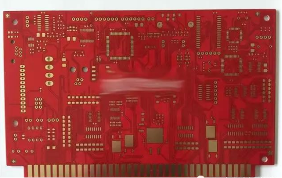
PTH is a very important step in the metallization process of printed circuit board holes. Its purpose is to form an extremely thin conductive copper layer on the hole wall and copper surface, preparing for subsequent electroplating. The hole in the hole wall coating is one of the common defects in the metallization of printed circuit boards, and it is also one of the projects that can easily cause batch scrapping of printed circuit boards. Therefore, solving the problem of hole in the printed circuit board coating is a key control for printed circuit board manufacturers. However, due to the diverse reasons for its defects, only by accurately judging the characteristics of its defects can effective solutions be found.


