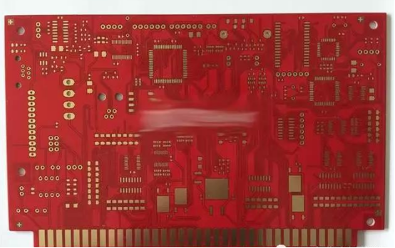
There are several treatment processes for the surface of the circuit board: light board (without any treatment on the surface), rosin board, OSP (organic solder protective agent, slightly better than rosin), tin spraying (with or without lead tin), gold-plated board, gold-plated board, etc. These are more visible.
Let’s briefly introduce the difference between gold plating and gold deposition.

The difference between gold deposition process and gold plating process:
The method of chemical deposition is used to deposit gold. A layer of coating is generated by chemical oxidation and reduction reaction, which is generally thicker. It is one of the methods of chemical nickel gold deposit, and can reach a thicker gold layer.
Gold plating adopts the principle of electrolysis, also known as electroplating. Other metal surface treatment also mostly adopts electroplating.
In practical product applications, 90% of the gold plates are sunk gold plates, because the poor weldability of the gold plate is his fatal defect, and it is also the direct reason that many companies give up the gold plating process!
Gold deposition process deposits nickel and gold coating with stable color, good brightness, flat coating and good weldability on the surface of printed circuit. Basically, it can be divided into four stages: pretreatment (degreasing, micro-etching, activation and post-leaching), nickel precipitation, gold precipitation, and post-treatment (waste gold washing, Dl washing, and drying). The thickness of gold deposit is between 0.025-0.1um.
Gold should be used for surface treatment of circuit boards because of its strong conductivity, good oxidation resistance and long service life. It is generally used for key boards, gold finger boards, etc. The most fundamental difference between gilded and gilded plates is that gilded is hard gold (wear-resistant) and gilded is soft gold (non wear-resistant).
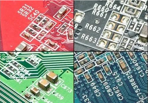
1.The crystal structure formed by gold deposition is different from that of gold plating. The thickness of gold deposition is much thicker than that of gold plating. The gold deposition will be golden yellow and more yellow than that of gold plating (this is one of the methods to distinguish between gold plating and gold deposition), and the gold plating will be slightly white (the color of nickel).
2.The crystal structure formed by gold deposition is different from that of gold plating. Compared with gold plating, gold deposition is easier to weld and will not cause poor welding. The stress of the sink plate is easier to control, which is more conducive to the processing of Bonding products. At the same time, because the gold plate is softer than the gold plate, the gold finger made of the gold plate is not wear-resistant (the disadvantage of the gold plate).
3.There is only nickel and gold on the pad of the sink plate, and the signal transmission in the skin effect is in the copper layer, which will not affect the signal.
4.The crystal structure of precipitated gold is more dense than that of gold plating, and it is not easy to produce oxidation.
5.With the increasing requirements for the processing accuracy of circuit boards, the line width and spacing have reached below 0.1mm. Gold plating is easy to cause gold wire short circuit. There is only nickel gold on the pad of the sink plate, so it is not easy to produce short circuit of gold wire.
6.There is only nickel gold on the pad of the sink plate, so the combination of resistance welding and copper layer on the line is stronger. The project will not affect the spacing when making compensation.
7.For the boards with higher requirements, the flatness requirements are better. Generally, the sinking gold is used. Generally, the black pad after assembly will not appear after the sinking gold. The flatness and service life of the gold-plated plate are better than that of the gold-plated plate.


 Oct. 10, 2020