Tin spraying is the process of soaking a circuit board in molten tin and lead. When sufficient tin and lead are adhered to the surface of the power circuit board, warm air is used to charge and scrape off the excess tin and lead. After tin lead cooling, the area where the circuit board is soldered will be coated with a moderately thin layer of tin lead, which is the rough process of tin spraying manufacturing. The surface treatment technology of PCB is currently commonly used in the tin spraying process, also known as Hot air solder leveling technology, which involves spraying a layer of tin on the solder layer to improve the turn-off characteristics and malleability of the PCB solder layer.
As a common surface coating method for PCB circuit boards, tin spraying SMOBC&HAL is widely used in production and manufacturing. The quality of tin spraying immediately affects the quality of welding and soldering for future customers. Therefore, the quality of tin spraying has become a key aspect of quality management for PCB circuit board manufacturers, targeting general single panels. Tin spraying and OSP processing processes are widely used, while resin processing processes are widely used on single-layer PCBs, and gold plating processes are used on circuit boards that must be bound with ICs. Sinking gold is more commonly used on plug-in boards.
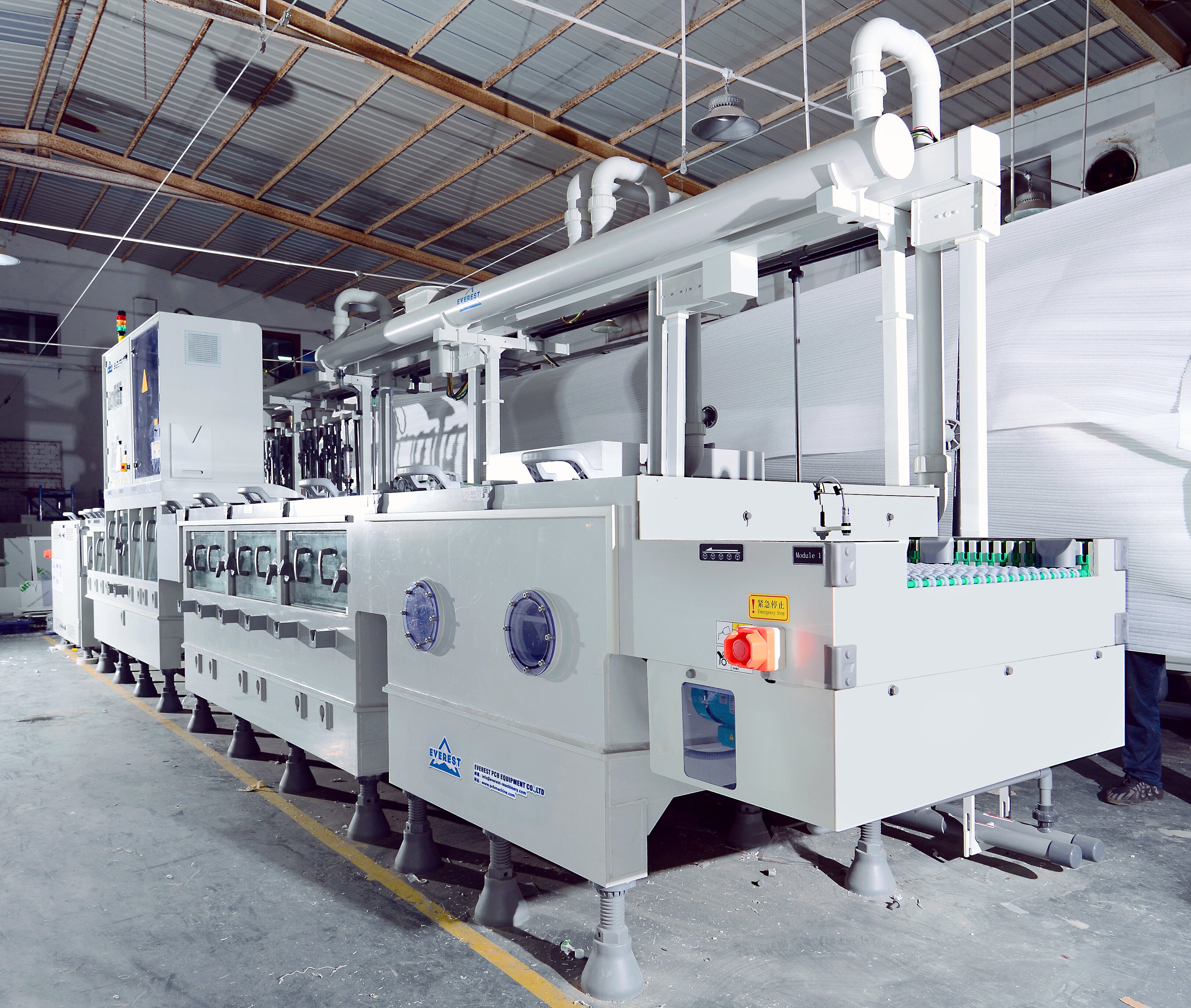
The production process of PCB tin spraying mainly includes: laying out the board (applying electroplated power plug maintenance tape) – solving before heating and leveling – heating and leveling – cleaning after heating and leveling – inspection.
Although the overall processing process is simple, there are many technical standards that must be grasped in order to produce high-quality and compliant PCB circuit boards with warm air, such as welding material temperature, gas knife cyclone temperature, gas knife working pressure, immersion welding time, and improving strength. This situation all has ratings, but during work, it is necessary to change according to the external standards of PCB circuit boards and the regulations of production and processing orders, such as board thickness and length. Different single-layer, double-sided, solid wood multi-layer board. The prerequisites they use are different. Only by understanding and grasping the main parameters of various processing techniques, and adjusting the equipment carefully, delicately, and effectively according to the different types and regulations of PCB circuit boards, can we warm and level out PCB circuit boards that meet the standards.
The primary efficacy of PCB tin spraying:
(1)Prevent air oxidation of bare copper surfaces; Copper is very prone to air oxidation in the air, leading to non conductivity of the PCB solder layer or reducing repair welding characteristics. Based on tin coating on the copper surface, reasonable copper surface and gas protection can be used to maintain the conductivity and malleability of the PCB.
(2)Maintain solder wire properties; Other metal surface treatment methods also include: hot melting, organic chemical protective film OSP, organic chemical tin, organic chemical silver, chemical nickel gold, electroplating process nickel gold, etc; However, it is best to consider the high cost-effectiveness of tin sprayed PCB boards due to their processing characteristics. Tin sprayed PCB boards contain copper tin double layer metal materials that can adapt to weaker standards in new environments and have good soldering wire characteristics, which are more integrated in high temperature and corrosive conditions.
This type of board is widely used in industrial production control systems, communication equipment, and national defense machinery equipment. The advantage of spray tin PCB is that in daily PCB surface treatment, the spray tin processing process is known as the best malleability. Due to the presence of tin on the solder layer, in the case of electric welding with tin, it looks very easy compared to the electroplating gold plate or resin and OSP processing process. This is very easy for everyone to solder by hand, and electric welding looks very easy.

 Sep. 13, 2022