OSP is a process for surface treatment of copper foil on printed circuit boards (PCBs) that meets the RoHS directive requirements. OSP is the abbreviation for Organic Solderability Preservatives. Simply put, OSP is the chemical process of growing an organic film on a clean bare copper surface. This film has oxidation resistance, heat shock resistance and moisture resistance to protect the copper surface from further rusting (oxidation or vulcanization, etc.) in normal environment; However, in the subsequent high welding temperature, this protective film must be easily removed by flux, so that the exposed clean copper surface can be immediately combined with molten solder to form a solid solder joint in a very short time.
OSP has three major categories of materials: rosin, active resin, and azole. Currently, the most widely used is the oxazole OSP. The oxazole OSP has been improved for about 5 generations, named BTA, IA, BIA, SBA, and the latest APA.
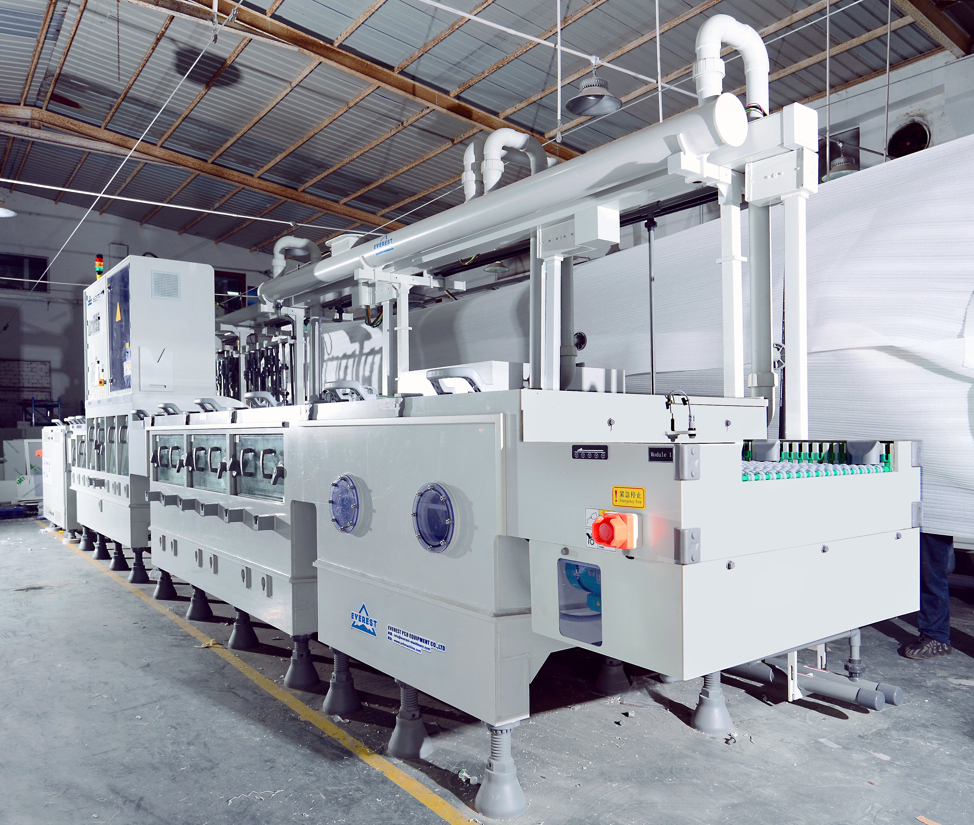
The process of OSP is: degreasing ->secondary water washing ->micro etching ->secondary water washing ->acid washing ->DI water washing ->film forming air drying ->DI water washing ->drying, which is relatively easy compared to other surface treatment processes. The purpose of micro etching is to form a rough copper surface for easy film formation. The thickness of micro etching directly affects the film forming rate, therefore, it is very important to maintain the stability of micro etching thickness in order to form a stable film thickness
- Degreasing
The effectiveness of oil removal directly affects the quality of film formation. Poor oil removal results in uneven film thickness. On the one hand, the concentration can be controlled within the process range by analyzing the solution. On the other hand, it is also necessary to regularly check whether the oil removal effect is good. If the oil removal effect is not good, the oil removal fluid should be replaced in a timely manner.
- Micro etching
The purpose of micro etching is to form a rough copper surface for easy film formation. The thickness of micro etching directly affects the film formation rate, therefore, it is very important to maintain the stability of micro etching thickness in order to form a stable film thickness. It is generally appropriate to control the micro etching thickness between 1.0 and 1.5um.
- Film-forming
It is best to use DI water for washing before film forming to prevent contamination of the film forming solution. It is also recommended to use DI water for washing after film formation, and the pH value should be controlled between 4.0 and 7.0 to prevent contamination and damage to the film layer. The key to the OSP process is to control the thickness of the anti oxidation film. The film is too thin and has poor thermal shock resistance. When passing reflow soldering welding, the film cannot withstand high temperature (190-200 ° C), which ultimately affects the welding performance. On the electronic assembly line, the film cannot be well dissolved by flux, affecting the welding performance. It is generally suitable to control the film thickness between 0.2 and 0.5um.
Disadvantages of OSP process:
OSP also has its shortcomings, such as the variety of actual formulas and varying performance. That is to say, the certification and selection of suppliers should be done well enough.
The drawback of the OSP process is that the protective film formed is extremely thin and prone to scratches (or abrasions), requiring careful operation and operation. At the same time, the OSP film (referring to the OSP film on the unwelded connection plate) that has undergone multiple high-temperature welding processes may discolor or crack, affecting solderability and reliability.
test
Using OSP surface treatment, if the test point is not covered by solder, it will lead to contact issues with the needle bed fixture during ICT testing. There are many human factors that can affect the effectiveness of ICT testing, including the type of OSP provider, the number of times it passes through the reflux furnace, whether it is a peak process, nitrogen reflux or air reflux, and the type of simulation testing used during ICT. Simply using a sharper probe type to pass through the OSP layer will only result in damage and puncture of PCA test vias or test pads. Therefore, it is strongly recommended not to directly detect exposed copper solder pads, and it is required to consider adding tin to all test points when opening the steel mesh.
Application Guide
The solder paste printing process needs to be mastered well, as poorly printed boards cannot be cleaned using IPA or other methods, which can damage the OSP layer.
The thickness of transparent and non-metallic OSP layers is also difficult to measure, and the degree of transparency on the coating coverage is also not easy to see. Therefore, it is difficult to evaluate the quality stability of suppliers in these aspects.
OSP technology does not have IMC isolation between Cu in the solder pad and Sn in the solder. In lead-free technology, SnCu in solder joints with high Sn content grows rapidly, affecting the reliability of the solder joints.
Packaging and storage
The organic coating on the surface of OSP PCB is extremely thin. If exposed to high temperature and high humidity for a long time, the PCB surface will be oxidized, and the solderability will become poor. After the reflow soldering process, the organic coating on the PCB surface will also become thin, resulting in easy oxidation of PCB copper foil. So the storage method and use of OSP PCB and SMT semi-finished boards should follow the following principles:
(a) OSP PCB incoming materials should be vacuum packaged and accompanied by desiccants and humidity display cards. During transportation and storage, isolation paper should be used between PCBs with OSP to prevent friction damage to the OSP surface.
(b) Do not expose to direct sunlight, maintain a good warehouse storage environment, with a relative humidity of 30-70%, a temperature of 15-30 ℃, and a shelf life of less than 6 months.
(c) When unpacking at SMT site, it is necessary to check the humidity display card and go online within 12 hours. Never open multiple packages at once. In case it cannot be completed or if there is something wrong with the equipment, it will take a long time to solve, which can easily lead to problems. After printing, do not stay in the furnace as soon as possible, because the flux in the solder paste has strong corrosion on the OSP film. Maintain a good workshop environment: relative humidity of 40-60%, temperature of 22-27 ℃. During the production process, it is necessary to avoid direct contact with the surface of the PCB by hand to avoid oxidation caused by sweat contamination on the surface.
(d) After the completion of SMT single sided mounting, the second SMT component mounting assembly must be completed within 24 hours.
(e) After completing the SMT, complete the DIP plugin as soon as possible (up to 36 hours).
(f) OSP PCBs cannot be baked, as high-temperature baking can easily cause color change and deterioration of OSP.

 Nov. 09, 2021