
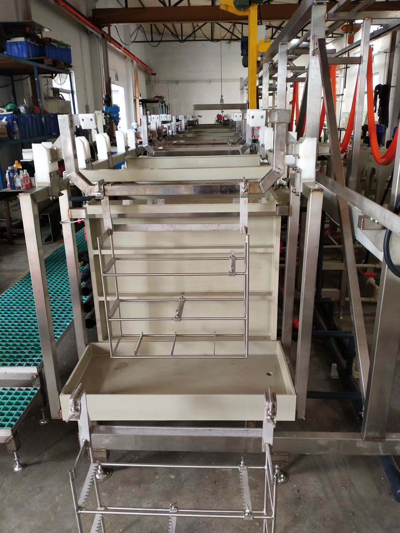
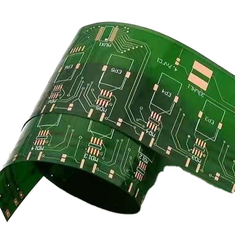
PTH is a very important step in the metallization process of printed circuit board holes. Its purpose is to form an extremely thin conductive copper layer on the hole wall and copper surface, preparing for subsequent electroplating. The hole in the hole wall coating is one of the common defects in the metallization of printed circuit boards, and it is also one of the projects that can easily cause batch scrapping of printed circuit boards. Therefore, solving the problem of hole in the printed circuit board coating is a key control for printed circuit board manufacturers. However, due to the diverse reasons for its defects, only by accurately judging the characteristics of its defects can effective solutions be found.
1. Hole wall coating voids caused by PTH
(1) Copper content of PTH, concentration of sodium hydroxide and formaldehyde
The solution concentration of the copper cylinder is the first consideration. Generally speaking, the copper content, sodium hydroxide and formaldehyde concentration are proportional. When any of them is lower than 10% of the standard value, the balance of chemical reaction will be broken, resulting in poor PTH and dotted cavities. Therefore, priority should be given to adjusting the parameters of various chemicals in the copper cylinder.
(2) Temperature of tank liquid
The temperature of the tank solution also has an important impact on the activity of the solution. There are generally temperature requirements in each solution, some of which require strict control. So the temperature of the tank liquid should also be monitored at all times.
(3) Control of activation solution
Low divalent tin ions can cause the decomposition of colloidal palladium and affect its adsorption. However, as long as the activation solution is regularly added and supplemented, it will not cause major problems. The key to controlling the activation solution is that it cannot be stirred with air. Oxygen in the air will oxidize divalent tin ions, and water cannot enter, which will cause the hydrolysis of SnCl2.
(4) Cleaning temperature
The cleaning temperature is often overlooked, and the optimal temperature for cleaning is above 20 ℃. If it is below 15 ℃, it will affect the cleaning effect. In winter, the water temperature becomes very low, especially in the north. Due to the low temperature of water washing, the temperature of the board after cleaning will also become very low. After entering the copper cylinder, the temperature of the board cannot immediately rise, which will affect the deposition effect due to missing the golden time of copper deposition. So in places with low ambient temperatures, it is also important to pay attention to the temperature of the cleaning water.
(5) Temperature, concentration, and time of use of pore forming agents
The temperature of the chemical solution has strict requirements. Excessive temperature can cause the decomposition of the pore forming agent, lower the concentration of the pore forming agent, and affect the effect of pore forming. Its obvious feature is the appearance of dot shaped voids at the glass fiber cloth inside the hole. Only by properly coordinating the temperature, concentration, and time of the drug solution can a good pore forming effect be achieved while also saving costs. The continuous accumulation of copper ion concentration in the chemical solution must also be strictly controlled.
(6) Temperature, concentration, and time of use of reducing agents
The role of reduction is to remove the residual Potassium manganate and Potassium permanganate after drilling. Uncontrolled parameters of the liquid medicine will affect its role. Its obvious feature is that there are dotted cavities at the resin in the hole.
(7) Vibration and sway
Vibration and uncontrolled swaying can cause circular voids, mainly due to the failure to eliminate bubbles in the holes, with small orifice plates with high thickness to diameter ratios being the most obvious. Its obvious feature is that the cavities inside the holes are symmetrical, while the copper thickness in the parts with copper inside the holes is normal, and the graphic electroplating coating (secondary copper) wraps the entire plate coating (primary copper).
2.Hole wall coating voids caused by pattern transfer
The voids in the hole wall coating caused by pattern transfer are mainly annular voids at the hole opening and annular voids in the hole. The specific reasons for their occurrence are as follows:
(1) Pretreatment brush board
(2) Residual adhesive at the orifice
(3) Pretreatment Microetching
3.Hole wall coating voids caused by graphic electroplating
(1) Pattern Electroplating Microetching
The micro etching amount of graphic electroplating should also be strictly controlled, and the defects generated are basically the same as the micro etching before dry film treatment. In severe cases, the hole wall will have a large area without copper, and the thickness of the entire board layer on the board surface will be significantly thinner. So it is best to optimize the process parameters by conducting DOE experiments to regularly measure the micro erosion rate.
(2) Poor dispersion of tin plating (lead tin)
Due to factors such as poor solution performance or insufficient swing, the thickness of the tin plating layer is insufficient. During subsequent film removal and alkaline etching, the tin and copper layers in the middle of the hole are eroded, resulting in circular voids. Its obvious feature is that the thickness of the copper layer inside the hole is normal, there are obvious traces of etching on the fault edge, and the graphic electroplating layer does not
Wrap the entire board (see Figure 5). In response to this situation, some tin polishing agent can be added to the pickling before tin plating, which can increase the wettability of the board and increase the swing amplitude.
4.Conclusion
There are many factors that cause coating voids, the most common being PTH coating voids. By controlling the relevant process parameters of the solution, the generation of PTH coating voids can be effectively reduced. But other factors cannot be ignored. Only by carefully observing and understanding the causes of coating voids and the characteristics of defects can problems be solved in a timely and effective manner, and the quality of products be maintained. Due to my limited level of experience, I have listed some practical problems encountered in daily production for sharing and communication with peers.

 Sep. 08, 2022


