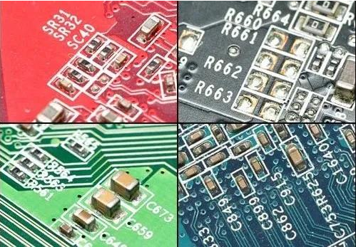
With the improvement of product performance, the PCB is also constantly updated and developed. The circuit is becoming more and more dense, and more and more components need to be placed. However, the size of the PCB will not become larger, but will become smaller and smaller. At this time, it requires considerable technology to drill holes on the plate.
There are many kinds of FCB drilling technology. The traditional method is to make the inner blind hole. When pressing the multilayer plate one by one, first use two double-sided plates with through holes as the outer layer, and press the inner plate with no holes to produce the glue-filled blind hole. The blind hole side of the outer plate is drilled mechanically. However, when making machine-drilled blind holes, it is not easy to set the drill depth, and the conical hole bottom affects the effect of mirror copper. In addition, the process of making the inner blind hole is too long and wastes too much cost, so the traditional method is increasingly unsuitable.
In addition to the carbon dioxide drilling and laser drilling we introduced earlier, the commonly used PCB microporous technology now includes mechanical drilling, photosensitive drilling, laser drilling, plasma etching and chemical etching.
Mechanical drilling is made by high-speed machining, the most important of which is the drill bit. The drill bit is generally made of tungsten-cobalt alloy, which is sintered at high temperature and high pressure with tungsten carbide powder as the matrix and cobalt as the binder. It has high hardness and high wear resistance, and can drill the required hole smoothly.
Laser hole forming is made by using carbon dioxide and ultraviolet laser cutting. The gas or light forms a beam of light, which has strong heat energy, and can burn through the copper foil to produce the required holes. The principle is the same as cutting, mainly controlling the beam.
Plasma, also known as plasma, is composed of particles with large spacing, which are in irregular continuous collision, and its thermal motion is similar to that of ordinary gas. The etched hole of the plasma is mainly used for PCB of resin copper layer. The oxygen-containing gas is used as the plasma. After contacting with the copper, the oxidation reaction will occur, and then the resin material will be removed to form the hole.
As mentioned earlier, the objects left on the PCB that cannot be cleaned by general methods can be cleaned by chemical cleaning method to make the chemical agent react with the residue. The same is true for drilling holes. The copper foil, resin, etc. can be eroded by dropping chemical agents at the place where drilling is needed, and finally the holes can be formed.

 Sep. 08, 2022