
Hot air leveling is to immerse the printed circuit board into the molten solder (63Sn / 37Pb), and then blow off the excess solder on the surface of the printed circuit board and in the metallization hole with hot air to obtain a smooth, uniform and bright solder coating layer. After hot air leveling, the lead tin alloy coating on the surface of printed circuit board shall be bright, uniform and complete, with good weldability, no nodulation, no semi wetting, and no exposed copper. Copper exposure on the surface of pad and metallization hole after hot air leveling is an important defect in finished product inspection. It is one of the common causes of hot air leveling rework. There are many reasons for this problem, including the following.
1. Insufficient pretreatment and poor coarsening.
The quality of PCB hot air leveling pretreatment process has a great impact on the quality of hot air leveling. In this process, the oil stain, impurities and oxide layer on the pad must be completely removed to provide fresh solderable copper surface for tin dipping. At present, the more commonly used pretreatment process is mechanical spraying. First, sulfuric acid hydrogen peroxide micro etching, pickling after micro etching, then water spraying and flushing, hot air drying, spraying flux and hot air leveling immediately. The copper exposure caused by poor pretreatment occurs in large numbers at the same time regardless of types and batches. The copper exposure points are often distributed on the whole plate surface, especially on the edge. Using a magnifying glass to observe the pretreated circuit board, it will be found that there are obvious residual oxidation spots and stains on the pad. In case of similar situations, chemical analysis shall be carried out for the micro etching solution, check the second pickling solution, adjust the concentration of the solution, replace the solution with serious pollution due to long service time, and check whether the spray system is unobstructed. Appropriately prolonging the treatment time can also improve the treatment effect, but attention should be paid to the over corrosion phenomenon. After the reworked circuit board is leveled by hot air, the treatment line is treated in 5% hydrochloric acid solution to remove the oxide on the surface.
2. The surface of the pad is not clean, and there is residual solder resist polluting the pad.
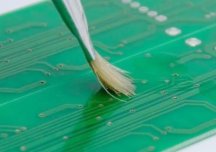
At present, most manufacturers use full board screen printing liquid photosensitive solder resist ink, and then remove the excess solder resist through exposure and development to obtain the time solder resist pattern. In this process, poor control of pre drying process, too high temperature and too long time will cause difficulties in development. Whether there are defects on the solder resist film, whether the composition and temperature of the developer are correct, whether the development speed, that is, whether the development point is correct, whether the nozzle is blocked, whether the pressure of the nozzle is normal, and whether the water washing is good. Any of these conditions will leave residues on the pad. For example, the exposed copper formed due to the negative film is generally regular and at the same point. In this case, the use of a magnifying glass can find traces of solder resist substances at the exposed copper. In PCB design, a post should be set up to check the graphics and metallization holes before the curing process, so as to ensure that the pads and metallization holes of the printed circuit board sent to the next process are clean and free of solder resist ink residue.
3. Insufficient flux activity
The function of flux is to improve the wettability of copper surface, protect the laminate surface from overheating, and provide protection for solder coating. If the flux activity is not enough and the copper surface wettability is not good, the solder can not completely cover the pad. The copper exposure phenomenon is similar to the poor pretreatment. Prolonging the pretreatment time can reduce the copper exposure phenomenon. The current flux is almost all acidic flux, which contains acidic additives. If the acidity is too high, copper biting will be serious, resulting in high copper content in solder and rough lead and tin; If the acidity is too low, the activity is weak, which will lead to copper exposure. If the copper content in the lead tin bath is large, remove the copper in time. The selection of a stable and reliable flux by process technicians has an important impact on hot air leveling. Excellent flux is the guarantee of hot air leveling quality.

 Oct. 10, 2020


