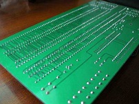
1. Brush plate
For the materials provided in the previous process (i.e. production board), the board surface shall be free of serious oxidation, oil stain and wrinkle.We use pickling (5% sulfuric acid) spray to remove organic and inorganic impurities, and then use 500 mesh nylon brush roller to grind and brush.After brushing, the copper surface shall be free of oxidation, the copper surface shall be uniformly roughened, the copper surface shall have strict flatness, and there shall be no trace on the copper surface.This effect enhances the adhesion between the wet film and the surface of copper foil to meet the requirements of subsequent processes.The surface state of copper foil after brushing directly affects the yield of PCB.
2. Screen printing
In order to achieve the required thickness of wet film, select the screen before silk screen printing, and pay attention to the thickness and mesh of the screen (i.e. the number of lines per unit length).The film thickness is related to the ink penetration of the screen. The theoretical ink penetration (uth) of the ink is: uth = dw2 \ (W + D) 2×1000 (D – net sand thickness d – wire diameter W – opening width)
The actual ink penetration is also related to the wet film viscosity, glue scraping pressure and glue scraping moving speed. In order to achieve uniform coverage, the scraper mouth should be bremsstrahlung.The thickness of the press film should be controlled at 15-25.μM, the film is too thick, which is easy to cause insufficient exposure, poor development, difficult to control pre drying, easy to cause battlefield films and difficult to operate.If the film is too thin, it is easy to produce overexposure, good corrosion resistance, poor insulation during electroplating, and difficult to remove the film.Manufacturing 0.15μFine lines below m shall be less than 20 after filmμm.
The viscosity of the wet film shall be adjusted before use, fully stirred and kept still for 15 minutes. The environment of the screen printing room shall be kept clean to prevent foreign matters from falling on the surface and affecting the qualified rate of the board. The temperature shall be controlled at about 20 ℃ and the relative humidity shall be about 50%.
3. Pre drying
Pre drying parameters: bake the first side at 80-100 ℃ for 7-10 minutes and the second side at 80-100 ℃ for 10-20 minutes.Pre drying is mainly to evaporate the solvent in the ink. Pre drying is related to the success or failure of wet film application.Insufficient pre drying, easy to stick the plate during storage and handling, and easy to stick the negative film during exposure, resulting in wire breakage or short circuit;Excessive pre drying, easy to develop unclean, and the line edge is serrated. Pre drying directly affects the quality of PCB, so it is important in normal operation, often test the wet film thickness, adjust the parameters of the oven according to the change of ambient temperature, and often check whether the air blowing and circulation system of the oven are good.The dried board should be exposed as soon as possible, preferably no more than 12 hours.
4. Exposure
Exposure is a photopolymerization process in which monomer molecules in the wet film absorb light energy under the action of ultraviolet light.High power exposure machine is selected to reduce exposure time and heat accumulation, ensure the stability of exposure graphics and reduce film sticking.Each shift shall keep the exposure room clean to avoid trachoma, gap and broken line caused by sundries adhering to the layout. Make an exposure ruler to adjust the exposure time to avoid excessive or insufficient exposure. Finally, the exposure level shall be controlled between 6-8 levels.During exposure, the same printed board shall be exposed at the same position as far as possible to ensure the same energy of the same board.If the exposure is too large, the effect of anti etching and anti electroplating is good, but the film removal effect is not ideal, the graphic line is reduced (positive film) or expanded (negative film), and the exposure is insufficient, resulting in poor development, poor corrosion resistance, hairy line edges, increased or reduced line spacing, which is easy to cause short circuit or wire breakage during etching.
5. Development
Development is the process of removing the unexposed wet film to obtain the required circuit pattern.Strictly control the concentration (10-12g / L) and temperature (30-34 ℃) of the developer. If the concentration of the developer is too high or too low, it is easy to cause unclean development.Optimize the development speed to match the exposure, and often clean the nozzle to make the pressure and distribution of the nozzle consistent.If the development time is too long or the development temperature is too high, the wet film surface will be degraded, and there will be serious permeability or side corrosion during electroplating or acid etching, which reduces the accuracy requirements of pattern making.
6. Etching and film removal
The circuit pattern we need is finally obtained by etching. The etching solution can be alkaline ferric chloride, acidic copper chloride and ammonia.During etching, different etching speeds shall be used for different copper foil thickness, and the etching speed shall match the temperature and concentration of the etching solution. The nozzle of the etching machine shall be maintained frequently to maintain uniform distribution of pressure and spraying solution, otherwise, uneven etching and copper wire on the edge will be caused, which will affect the quality of PCB.

 Oct. 10, 2020