
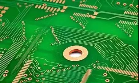
Blistering on the board surface of the circuit board is actually a problem of poor adhesion of the board surface. Further extension is the surface quality of the board surface, which includes two aspects:
1.Board surface cleanliness; Surface micro roughness (or surface energy).
All board surface blistering problems on circuit boards can be summarized as the above reasons.
The bonding force between the coatings is poor or too low, which is difficult to dry in the subsequent production, processing and assembly process. It can resist the coating stress, mechanical stress and thermal stress generated in the production and addition process, resulting in different degrees of separation between the coatings.

Some factors that may cause poor plate surface quality during production and processing are summarized as follows:
Problems in substrate processing:
Especially for some thin substrates (generally less than 0.8mm), it is not suitable to brush the plate with a plate brushing machine because of the poor rigidity of the substrate.
In this way, it may not be possible to effectively remove the protective layer specially treated to prevent the oxidation of the copper foil on the plate surface during the production and processing of the substrate. Although the layer is thin and the brush plate is easy to remove, it is difficult to adopt chemical treatment. Therefore, pay attention to control in the production and processing, so as not to cause the foaming problem on the plate surface caused by the poor adhesion between the copper foil on the plate surface and the chemical copper The problem is that when the thin inner layer is blackened, there will also be some problems, such as poor blackening and browning, uneven color, and poor local black browning.
2. Oil stain or other liquid contamination, dust pollution and poor surface treatment caused by plate surface machining (drilling, lamination, edge milling, etc.).
3. Poor copper brush plate:
The excessive pressure of the grinding plate before copper deposition causes the deformation of the orifice, and the copper foil fillet base at the orifice is brushed out to the leakage base material at the orifice. In this way, the foaming phenomenon at the orifice will be caused in the process of copper deposition, electroplating, tin spraying and welding. Even if the brush plate does not cause the leakage base material, the heavy brush plate will increase the roughness of the copper at the orifice. Therefore, the copper foil is very easy to produce excessive coarsening in the process of micro corrosion coarsening, which will also exist Therefore, attention should be paid to strengthening the control of the brush plate process, and the brush plate process parameters can be adjusted to the best through wear mark test and water film test;
4. Washing problem:
Because the copper plating treatment needs a lot of chemical liquid treatment, there are many kinds of acid-base, non-polar organic and other pharmaceutical solvents, and the plate surface is not washed cleanly. In particular, the copper plating adjustment degreaser will not only cause cross pollution, but also cause some defects such as poor local treatment or poor treatment effect and uneven defects on the plate surface, resulting in some problems in adhesion; therefore, attention should be paid to strengthening the water washing The control mainly includes the control of cleaning water flow, water quality, washing time, and plate dripping time; especially in winter, when the temperature is low, the washing effect will be greatly reduced, so we should pay more attention to the control of washing;
5. Micro etching in copper deposition pretreatment and pattern electroplating pretreatment:
Excessive micro etching will cause leakage of base material around the orifice and blistering around the orifice; insufficient micro etching will also cause insufficient bonding force and blistering; therefore, it is necessary to strengthen the control of micro etching; generally, the micro etching depth of copper deposition pretreatment is 1.5-2 microns, and the micro etching depth of pattern electroplating pretreatment is 0.3-1 microns. If possible, it is best to control the micro etching thickness by chemical analysis and simple test weighing method Corrosion rate: generally, the plate surface after micro etching has bright color, uniform pink and no reflection; if the color is uneven or there is reflection, it indicates that there are potential quality hazards in the pre-processing of the manufacturing process; pay attention to strengthen the inspection; in addition, the copper content, bath liquid temperature, load and micro etchant content of the micro etching tank should be paid attention to;
6.Poor rework of copper deposit:
Some reworked plates after copper deposition or pattern conversion will cause blistering on the plate surface due to poor fading plating, wrong rework method, improper control of micro corrosion time in the rework process or other reasons; if copper deposition is found on the line during the rework of copper deposition plate, it can be directly removed from the line after water washing and then pickled without corrosion; it is best not to re remove oil and micro corrosion; for For the plates that have been electrically thickened, the micro etching groove should be used for root plating. Pay attention to the time control. You can roughly calculate the stripping time with one or two plates to ensure the root plating effect; after the stripping, apply a group of soft grinding brushes behind the brushing machine, and then sink copper according to the normal production process, but the micro etching time should be halved or adjusted as necessary;
7.Oxidation of plate surface during production:
If the copper sinking plate is oxidized in the air, it may not only cause no copper in the hole, rough plate surface, but also cause blistering on the plate surface; if the copper sinking plate is stored in the acid solution for a long time, the plate surface will also be oxidized, and this oxide film is difficult to remove; therefore, the copper sinking plate shall be thickened in time in the production process, and the storage time shall not be too long. Generally, the copper plating shall be thickened within 12 hours at the latest;
8.The activity of copper precipitation solution is too strong:
The content of the three major components in the newly opened cylinder or tank liquid of the copper precipitation solution is too high, especially the high copper content will cause the defects of too strong activity of the tank liquid, rough chemical copper deposition, excessive inclusion of hydrogen, cuprous oxide and other defects in the chemical copper layer, resulting in the decline of the physical quality of the coating and poor adhesion; the following methods can be adopted appropriately: reduce the copper content (add pure water to the tank liquid) It includes three components: appropriately increasing the content of complexing agent and stabilizer, appropriately reducing the temperature of tank liquid, etc;
9.In the process of graphic transfer, insufficient water washing after development, too long storage time after development or too much dust in the workshop will cause poor board surface cleanliness and slightly poor fiber treatment effect, which may cause potential quality problems;
10.Organic pollution, especially oil pollution, occurs in the electroplating tank, which is more likely to occur for the automatic line;
11.Before copper plating, the pickling tank shall be replaced in time. Too much pollution in the tank liquid or too high copper content will not only cause the problem of plate surface cleanliness, but also cause defects such as plate surface roughness;
12.In addition, when the bath solution is not heated in the production of some factories in winter, special attention should be paid to the charged feeding of plates into the bath in the production process, especially the plating bath with air stirring, such as copper and nickel; for nickel cylinder, it is best to add a heated water washing bath before nickel plating in winter (the water temperature is about 30-40 ℃) to ensure the compactness and good initial deposition of nickel layer;
In the actual production process, there are many reasons for blistering on the board surface, and the author can only make a brief analysis. For the equipment technical level of different manufacturers, there may be blistering caused by different reasons. The specific situation should be analyzed in detail, and it is not allowed to generalize and copy mechanically; the above cause analysis is based on the production process, regardless of primary and secondary importance The series is just to provide you with a problem-solving direction and a broader vision. I hope it can play a role in your process production and problem-solving!

 Nov. 17, 2021


