
How to distinguish HDI PCB Primary pressing, Twice pressing and Triple pressing
HDI board (High Density Interconnector), namely high-density interconnection board, is a circuit board with High circuit distribution Density using micro blind hole embedding technology. The HDI board has an inner layer circuit and an outer layer circuit, and then uses drilling, hole metallization and other processes to connect the internal circuits of each layer.
HDI boards are generally manufactured by lamination method. The more times of lamination, the higher the technical level of boards. Ordinary HDI boards are basically stacked once. High order HDI boards use the stacking technology of twice or more, and advanced PCB technologies such as hole stacking, electroplating and hole filling, and laser direct drilling are also used.
When the density of PCB is increased to more than eight layers, the cost of HDI manufacturing will be lower than that of traditional complex pressing process. HDI board is conducive to the use of advanced construction technology, and its electrical performance and signal accuracy are higher than traditional PCB. In addition, HDI board has better improvement for radio frequency interference, electromagnetic wave interference, electrostatic discharge, heat conduction, etc.
Electronic products are constantly developing towards high density and high precision. The so-called “high” means not only improving the performance of the machine, but also reducing the size of the machine. High density integration (HDI) technology can make the terminal product design smaller, while meeting higher standards of electronic performance and efficiency. At present, many popular electronic products, such as mobile phones, digital cameras, laptops, automotive electronics, etc., use HDI boards. With the upgrading of electronic products and market demand, HDI boards will develop very rapidly.
Introduction to Common PCB
PCB (Printed Circuit Board), also known as printed circuit board in Chinese, is an important electronic component, a support for electronic components, and a carrier for electrical connection of electronic components. Because it is made by electronic printing, it is called “printed” circuit board.
Its main function is that after the electronic equipment adopts printed boards, due to the consistency of similar printed boards, the errors of manual wiring can be avoided, and electronic components can be automatically inserted or pasted, automatically soldered, and automatically detected, ensuring the quality of electronic equipment, improving labor productivity, reducing costs, and facilitating maintenance.
Are all PCB boards with blind buried holes called HDI boards?
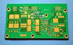
HDI boards are high-density interconnection circuit boards. The boards with blind hole electroplating and secondary pressing are HDI boards, which are divided into Primary pressing, second order, Triple pressing, fourth order, and fifth order HDIs. For example, the main board of iPhone 6 is a fifth order HDI.
Simple buried hole is not necessarily HDI. How HDIPCB Primary pressing, Twice pressingand Triple pressing distinguish Primary pressing is relatively simple, and the process and process are easy to control.
The Twice pressingproblems began to be troublesome. One was alignment, the other was punching and copper plating. There are many kinds of Twice pressingdesigns. One is stagger position of each order. When it is necessary to connect the next adjacent layer, it is connected in the middle layer through wires, which is equivalent to two Primary pressing HDIs.
The second is that the two Primary pressing holes overlap, and the Twice pressingis realized by overlapping. The processing is similar to the two Primary pressing holes, but there are many process points to be specially controlled, that is, the above mentioned.
The third method is to directly drill from the outer layer to the third layer (or N-2 layer). The process is different from the previous one, and the drilling is more difficult. For the Triple pressing, the Twice pressinganalogy is.
Differences between HDI board and ordinary PCB
The common PCB board is mainly FR-4, which is made of epoxy resin and electronic grade glass cloth. Generally, the traditional HDI uses adhesive backed copper foil on the outside. Because laser drilling cannot penetrate the glass cloth, it generally uses adhesive backed copper foil without glass fiber. However, the current high-energy laser drill can penetrate the 1180 glass cloth. This is no different from ordinary materials.

 Nov. 17, 2021


