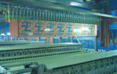
The purpose of pattern electroplating is to increase the thickness of lines and holes (mainly the thickness of hole copper) to ensure its conductivity and other properties.
Work process:
Load — degrease — 2 cascade rinse — Micro etch — 2 cascade rinse — Pickling — Copper Plating — 2 cascade rinse — Pickling — Tin plating — 2 cascade rinse — Unload — Rack stripping — 2 cascade rinse — Load
Function of each tank:
1. Degrease
Remove the residue on the board surface to achieve the purpose of cleaning the copper surface.
2. Micro etch
Clean the copper surface, make the copper surface rougher, and enhance the adhesion of the copper layer during copper plating.
3. Pickling (before copper plating)
Clean the plate surface to prevent sundries and water from entering the copper tank, reduce the chance of contamination of the solution in the copper plating tank, and prolong the service life of the copper tank.
4. Copper plating
A layer of copper shall be plated in the line and hole as required. In order to ensure the uniform thickness of the copper layer in the hole, vibration and swing must be added to the copper tank.
5. Pickling ( before tin plating)
Remove the residual copper ions on the plate, activate the copper surface and reduce the pollution of tin plating cylinder.
6. Tin plating
A layer of tin is plated on the circuit and hole as a protective layer during etching.
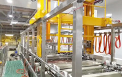
7. Rack stripping
Remove the metal (cu/sn) from the plating racks.

 Jun. 13, 2022