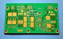
Function of copper clad on PCB
1. Copper clad on PCB can play a certain role in reflow. Of course, if there are many layers and the layer setting is reasonable, the role of copper clad reflow is very small.
2. PCB copper-clad can play a certain shielding role. Imagine the two copper-clad planes at the upper and lower layers as infinity to become a shielding box. Copper-clad can never do this, just like a chassis.
3.The PCB is coated with copper to reduce the ground wire impedance and improve the anti-interference ability.
4. Copper clad PCB reduces voltage drop and improves power efficiency.
5. In addition, it is connected with the ground wire to reduce the loop area.
Thickness of copper foil on PCB
1. Generally, the thickness of copper foil (copper clad) of single and double-sided PCB is about 35um (1.4mil).
2. Another specification is 50um, which is not common.
3. the surface layer of multilayer board is generally 35um (1.4mil), and the inner layer is 17.5um (0.7mil).
4. The thickness of copper foil can also be expressed in OZ. 1OZrefers to the thickness of copper uniformly covered by 1oz over an area of 1 square foot, that is, about 1.4mil.
Precautions when cladding copper on PCB
1. The method of single point connection in different places is to connect through 0 Ω resistance or magnetic bead or inductance;
2. The crystal oscillator in the circuit is a high-frequency emission source, which is coated with copper around the crystal oscillator, and then the shell of the crystal oscillator is grounded separately.
3. If the island (dead zone) problem is very large, define a ground via and add it.

 Nov. 09, 2021