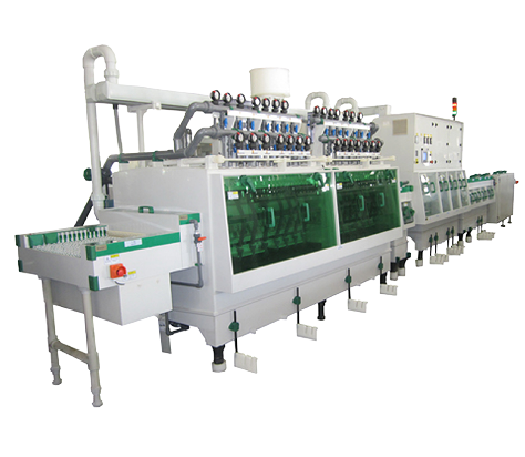
The process of printed circuit board from optical board to showing circuit pattern is a complex physical and chemical reaction process. This paper analyzes the last step – etching. At present, the typical process of printed circuit board (PCB) processing is “graphic electroplating”. That is, a layer of lead tin anti-corrosion layer is pre plated on the copper foil to be retained on the outer layer of the board, that is, the graphic part of the circuit, and then the rest of the copper foil is chemically corroded, which is called etching.
Type of etching:
It should be noted that there are two layers of copper on the board when etching. In the outer layer etching process, only one layer of copper must be completely etched, and the rest will form the final required circuit. This type of pattern plating is characterized in that the copper plating layer only exists below the lead tin corrosion resistant layer.
Another process is that the whole board is plated with copper, and the parts other than the photosensitive film are only tin or lead tin corrosion resistant layers. This process is called “full plate copper plating process”. Compared with pattern plating, the biggest disadvantage of copper plating on the whole board is that copper must be plated twice everywhere on the board, and they must be corroded during etching. Therefore, when the wire width is very fine, a series of problems will occur. At the same time, side corrosion will seriously affect the uniformity of lines.
In the processing technology of the outer circuit of the printed board, another method is to use the photosensitive film instead of the metal coating as the anti-corrosion layer. This method is very similar to the inner layer etching process. You can refer to the etching in the inner layer manufacturing process.
At present, tin or lead tin is the most commonly used resist layer, which is used in the ammonia etchant etching process Ammonia etchant is a widely used chemical solution, which has no chemical reaction with tin or lead tin. Ammonia etchant mainly refers to ammonia water / ammonia chloride etching solution.
In addition, ammonia water / ammonia sulfate etching solution can be purchased on the market. The copper in the sulfate based etching solution can be separated by electrolysis after use, so it can be reused. Because of its low corrosion rate, it is rarely seen in actual production, but it is expected to be used in chlorine free etching.
Someone tried to use sulfuric acid hydrogen peroxide as an etchant to etch the outer pattern. Due to many reasons including economy and waste liquid treatment, this process has not been widely used in the commercial sense Furthermore, sulfuric acid hydrogen peroxide cannot be used to etch the lead tin resist layer, and this process is not the main method in the production of PCB outer layer, so most people rarely pay attention to it

 Nov. 09, 2021