In order to ensure the production quality of PCB board, the manufacturer has experienced a variety of inspection methods in the production process, and each inspection method is aimed at different PCB board defects.
Basically, it can be divided into two categories: electrical test method and visual test method.
Electrical tests usually measure the impedance characteristics between test points to detect all continuity (i.e. open circuit and short circuit).Visual test finds defects by visually checking the characteristics of electronic components and printed circuits. Electrical testing is more accurate when looking for short circuit or open circuit defects.Visual testing makes it easier to detect incorrect gaps between conductors. Visual inspection is usually carried out early in the production process. Try to find defects and repair them to ensure the highest product qualification rate.
Common inspection methods for PCB board are as follows:
1. Manual visual inspection of PCB board
Using a magnifying glass or calibrated microscope, the operator’s visual inspection determines whether the circuit board is qualified and when correction operation is required.This is the most traditional inspection method.Its main advantages are low initial cost and no test fixture, but its main disadvantages are subjective human error, high long-term cost, discontinuous defect detection and difficult data collection.At present, due to the increase of PCB production and the reduction of wire spacing and component volume on PCB, this method becomes more and more infeasible.
2. PCB online test
Identify manufacturing defects through electrical performance testing and test analog, digital and mixed signal components to ensure that they meet specifications.There are several test methods, such as needle bed tester and flying needle tester.The main advantages are low test cost of each board, powerful digital and functional test function, fast and complete short circuit and open circuit test, programming firmware, high defect coverage and easy programming.The main disadvantages are the need for test fixtures, programming and debugging time, high manufacturing cost and difficult to use.
3. PCB function test
Functional system test is a comprehensive test of the functional modules of the circuit board using special test equipment at the middle and end of the production line to confirm the quality of the circuit board.Functional testing is the earliest principle of automatic testing.It is based on specific boards or specific units and can be completed using various devices.There are final product testing, the latest physical model and stack testing.Functional testing usually does not provide in-depth data (such as pin position and component level diagnosis) to improve the process, but requires special equipment and specially designed test procedures.Writing function test program is very complex, so it is not suitable for most circuit board production lines.
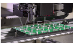
4. Automatic optical inspection
It is also called automatic appearance inspection. It is based on optical principle, and comprehensively uses image analysis, computer and automatic control technology to detect and deal with defects encountered in production.This is a relatively new method to identify manufacturing defects.AOI is usually used before and after reflux and before electrical test to improve the qualification rate of electrical treatment or functional test.At this time, the cost of correcting defects is much lower than that after the final test, usually more than ten times.
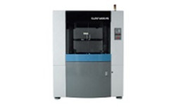
5. Automatic X-ray examination
Use the difference in X-ray absorptivity of different substances to check the parts to be tested and find defects.It is mainly used to detect defects in ultra-fine spacing and ultra-high density circuit boards, as well as bridge, chip loss, poor alignment and other defects during assembly.It can also use tomography technology to detect internal defects in IC chips.This is the only way to test the welding quality of ball grid array and solder ball.The main advantage is the ability to detect BGA welding quality and embedded components without the cost of fixtures.This is a relatively new test method with remarkable effect.
6. Laser detection system
This is the latest development of PCB testing technology.It scans the printed board with a laser beam, collects all measured data, and compares the actual measured value with the preset qualified limit value.The technology has been verified on bare board and is being considered for assembly board testing.This speed is sufficient for mass production lines.Fast output, no fixed device and barrier free visual access are its main advantages;The initial cost is high, and the maintenance and use problems are its main disadvantages.
7. Dimensional inspection
Use a two-dimensional image measuring instrument to measure the position, length and width, position and other dimensions of the hole.Because PCB is a small, thin and soft product, contact measurement is easy to deform, resulting in inaccurate measurement.Two dimensional image measuring instrument has become the best high-precision dimension measuring instrument.The image measuring instrument can realize automatic measurement after programming, which not only has high measurement accuracy, but also greatly shortens the measurement time and improves the measurement efficiency.
To sum up, among the seven detection methods, optical inspection and X-ray inspection are the most popular in the market.

 Oct. 10, 2020