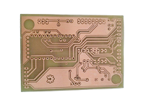
Large PCB manufacturers use electroplating and etching processes to produce wiring on the board. For electroplating, the production process begins with electroplated copper covering the outer plate substrate.
Photoresist etching is also used as another key step in the production of printed circuit boards. Protecting the copper required during etching requires a balance between removing unwanted copper and retaining the resist in place.The protection is carried out by coating a thin layer of resist (mainly composed of tin mixture) on the circuit pattern, so as to protect the required pattern from the influence of the etchant.
Since etching will remove excess copper from a clean blank plate, the thickness of copper plus coating cannot exceed the thickness of photoresist. First, the excess copper is removed, and then the subtraction process of removing the resist generates the circuit pattern.Although manufacturers can use buckets, water tanks or sprayers to apply etchant, most high-pressure spraying equipment can etch standard sized PCB designs in less than a minute.
Although etchant or stripping agents are usually classified as ammonia etchant, the general components usually include ammonia / ammonium chloride or ammonia / ammonium sulfate for spray etching.The resist prevents the etching solution from contacting the desired conductive pattern.Since the etchant does not affect the resist, only unwanted copper is removed.
In the etching process, the reaction between ammonia etchant and copper produces a large number of cuprous ions from the copper ions of copper. Excessive cuprous ions will form a dull and uneven coating on the coating and damage the conductivity.In order to cope with the overload of cuprous ions, the etching equipment sucks air into the etching chamber.The oxygen absorbed from the introduced gas stream will lead to the reoxidation of cuprous ions to copper ions.
Stripping the resist requires a process involving oxidation and reduction or redox reaction.When four electrons can be removed from the resist by nitric acid oxidation, the process will tarnish the copper and produce copper oxide.Reduction reduces the amount of oxidant by reducing the amount of oxygen that adds two electrons to copper.
The process begins by oxidizing to remove the resist and reducing to protect copper.The removal of tin requires complete oxidation, and then tin needs to be dissolved into the solution by using tin salt. Unfortunately, the consistency of copper is much softer than tin. As a result, copper will peel off before tin.The manufacturer uses inhibitors in the etchant to prevent copper oxidation from damaging the conductive surface of the PCB.
After completion, the function PCB shall not have etching quality problems. Otherwise, the PCB will not meet the specification requirements for consumer and industrial products.The manufacturer defines the etching quality according to the uniformity of the trace edge and the amount of etching undercut.Since the etchant can flow in any direction, including lateral and downward flow, the etchant will undercut traces.
When considering the quality of the plate, the manufacturer uses a formula called “etching coefficient”. The “etching factor” is equal to the undercut divided by the amount of copper etched. Undercutting can be minimized by configuring production equipment and adjusting etching chemistry through the use of bank agents.
In addition to preventing edge undercut, the manufacturer is also committed to protecting the production process from residual photoresist. Any un-stripped photoresist will leave copper feet near the routing, thus shortening the distance between the routing. In addition to preventing the accumulation of residual photoresist, manufacturers also try to minimize the accumulation of etchant on the plate surface. Etching agent agitation can allow different etching patterns to be formed on the PCB.

 Dec. 20, 2019