
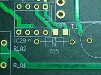
印刷电路板中的阻焊层显影工艺是印刷电路板所有工艺中相对简单的工艺,但它也起着重要作用。阻焊层显影工艺控制印刷板的外观和孔的内部,并努力使;漂亮的外套”;印刷电路板“;最美丽的”;,从而使印刷电路板看起来更舒适,保护和控制孔中的质量。阻焊层不会出现在印刷板的孔中,以确保印刷板的质量。因此,印刷电路板的阻焊层开发过程是一个非常重要的过程。下面将介绍PCB阻焊层的开发过程以及遇到的问题的解决方案。
印刷电路板中的阻焊显影工艺是在丝网印刷后用感光板覆盖印刷电路板上的焊盘,使其不会暴露在紫外线辐射下,紫外线辐射后阻焊保护层更牢固地附着在印刷电路板表面。焊盘不暴露在紫外线辐射下,因此在热空气整平过程中,铜焊盘可以暴露出铅和锡。
焊料掩模开发过程大致可分为三个操作步骤:
1.第一个程序是暴露。
首先,在曝光前检查曝光架的聚酯薄膜和玻璃框架是否清洁。如果它们不干净,请及时用防静电布擦拭。然后,打开曝光机的电源开关,然后打开真空按钮选择曝光程序。在正式曝光之前,曝光机可以是“;暴露在空气中”;五次,功能“;空气暴露”;是使机器进入饱和工作状态,最重要的是使紫外线曝光灯的能量进入正常范围。没有“;空气暴露”;,曝光灯的能量可能不会进入最佳工作状态。在曝光过程中,印刷电路板会出现问题。曝光机进入最佳工作状态。在对准照相底片之前,检查底片的质量是否合格。检查基板上的药物膜表面是否有针孔和外露部分,以及它们是否与印刷板的图形一致,因为这会检查照相基板,从而避免因一些不必要的原因返工或报废印刷板。
焊料掩模开发通常采用视觉定位,使用银盐基板,将基板的焊盘与印刷板的焊盘孔重叠对齐,并用胶带固定即可暴露。对齐过程中存在许多问题。例如,由于基板与温度和湿度等因素有关,如果温度和湿度控制不好,摄影基板可能会收缩或扩大变形。这样,在焊料掩模开发过程中,摄影基板与PCB焊盘并不完全一致。当基板减小时,请查看基板焊盘和印刷板焊盘之间的差异。如果差异很小,可以在热空气流平过程中施加铅和锡,那么就没有大问题,可以进行阻焊层开发。如果差异很大,只需再次复制,并尝试使底板垫重合。对齐前,注意基板的药物膜表面是否颠倒。在对齐过程中,确保药物膜表面朝下。如果面朝上,药物膜表面容易被划伤,导致基板暴露,使印刷板暴露部分存在耐焊性,这将严重造成印刷板的浪费。此外,还应该注意的是,有时化妆的底板会与印刷电路板的图形不一致。通常,化妆的底板会沿着化妆板的边缘切割,然后对齐后露出整个印刷板。在正式曝光和焊料掩模开发之前,应注意上述问题。
曝光前,检查印刷电路板是否被真空箱吸收。真空包层的压力应足够,无露水。如果暴露的空气会使紫外线沿着电路板侧面照射到图案中,导致遮光部分暴露,显影不会丢失。有时,它会暴露在一侧。在这种情况下,应使用黑布将一侧没有图案的一侧与曝光灯发出的紫外线隔开。如果不使用黑布,紫外线会通过没有图案的一侧进入焊盘,这样焊盘孔中的阻焊剂在曝光后就无法显影。当暴露两面图形不一致的印刷电路板时,先丝网印刷一面以防焊接,然后再暴露一面。显影后,在丝网印刷的另一面进行抗焊处理,因为如果两面同时进行丝网印刷和曝光,一侧会有更复杂的图形,需要屏蔽的焊盘更多,另一侧需要屏蔽的零件更少,这样紫外线就会从一侧照射到另一侧,遮光较多的一侧在紫外线照射后的显影过程中不会显示出来,这会导致返工或报废。在曝光过程中,丝网印刷后的印刷板在固化过程中没有干燥。在这种情况下,阻焊剂在对准过程中会粘在感光板上,印刷板也会被返工。因此,如果发现它没有干燥,特别是如果大多数印刷板没有干燥,应该在烤箱中再次干燥。这些情况都是暴露过程中容易出现的问题,所以我们应该仔细检查,及时发现并解决。
2.第二个过程是发展。
开发操作通常在开发人员中进行。通过控制显影剂温度、传输速度和喷雾压力等显影参数,可以获得更好的显影效果。开发是用开发溶液去除焊盘上的焊料电阻。用于显影的溶液是1%无水碳酸钠,液体温度通常在30至35摄氏度之间。在正式显影之前,应加热显影剂,使溶液达到预定温度,以达到最佳显影效果。显影机分为三个部分:第一部分是喷涂部分,主要使用高压注射无水碳酸钠来溶解未暴露的阻焊剂;第二部分是水洗部分。首先,使用高压泵清洗残留溶液,然后进入循环水进行彻底清洗;第三部分是干燥部分。干燥段前后有一个气刀,主要利用热风干燥板材。此外,如果干燥部分的温度很高,板也可以干燥。
正确的开发时间由开发点决定。开发难点必须保持在开发段总长度的恒定百分比。如果显影点离显影部分的出口太近,并且未暴露的阻焊层没有完全显影,则未暴露的抗焊层的残留物可能会留在板表面上。如果显影点离显影部分的入口太近,暴露的阻焊层可能会被蚀刻,并由于与显影剂的长时间接触而变得多毛并失去光泽。通常,发展点控制在40%以内;开发段总长度的60%。此外,应该注意的是,在开发过程中很容易划伤电路板。通常的解决方案是,在开发过程中,电路板放置操作员应戴手套,轻轻处理电路板。也有不同尺寸的印刷电路板。因此,尽量把尺寸相似的木板放在一起。放置电路板时,电路板之间应保持一定距离,以防止电路板在传输过程中拥挤,从而导致“;干扰”;以及其他现象。视频显示后,将印刷板放在木支架上。
3.第三道工序是补板。
修复电路板包括两个方面:一是修复图像的缺陷,二是去除与所需图像无关的缺陷。在修复板材的过程中,应注意戴旋转手套,防止手汗污染板材表面。常见的板材表面缺陷包括:漏印,也称为飞白、氧化、表面不平整、孔内电阻焊、图形有针孔、表面污垢、两侧颜色不一致、开裂、气泡和重影。在修改过程中,由于一些印刷电路板存在严重缺陷且无法修复,使用氢氧化钠水溶液加热并溶解原始阻焊层,然后在丝网印刷和曝光后进行返工。如果印刷电路板的缺陷很小,比如小铜点,可以用细刷仔细蘸取调整后的阻焊层。

 2021年10月15日


