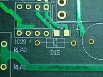
The solder resist development process in the printed board is a relatively simple process among all processes of the printed board, but it also plays an important role. The solder resist development process controls the appearance of the printed board and the inside of the hole, and strives to make the “beautiful coat” of the printed board “the most beautiful”, so as to make the printed board look more comfortable, protect and control the quality in the hole. The solder resist will not appear in the hole of the printed board to ensure the quality of the printed board. Therefore, the solder resist development process of the printed board is a very important process. The following will introduce the PCB solder resist development process and the solutions to the problems encountered.
The solder resist development process in the printed board is to cover the solder pad on the printed board with a photographic plate after screen printing, so that it will not be exposed to ultraviolet radiation, and the solder resist protective layer is more firmly attached to the printed board surface after ultraviolet radiation. The solder pad is not exposed to ultraviolet radiation, so that the copper pad can be exposed for lead and tin during hot air leveling.
The solder mask development process can be roughly divided into three operating procedures:
1. The first procedure is exposure.
First, check whether the polyester film and glass frame of the exposure frame are clean before exposure. If they are not clean, wipe them with an anti-static cloth in time. Then, turn on the power switch of the exposure machine, and then turn on the vacuum button to select the exposure procedure. Before formal exposure, the exposure machine can be “air exposed” for five times,The function of “air exposure” is to enable the machine to enter the saturated working state, and the most important thing is to make the energy of ultraviolet exposure lamp enter the normal range. Without “air exposure”, the energy of the exposure lamp may not enter the best working state. During exposure, the printed board will have problems.The exposure machine enters the best working state. Before aligning with the photographic plate, check whether the quality of the plate is qualified.Check whether there are pinholes and exposed parts on the drug film surface on the base plate, and whether they are consistent with the graphics of the printed board, because this will check the photographic base plate, so as to avoid rework or scrapping of the printed board for some unnecessary reasons.
Solder mask development usually adopts visual positioning, uses silver salt base plate, overlaps and aligns the pad of the base plate with the pad hole of the printed board, and can be exposed by fixing it with adhesive tape.There are many problems in alignment. For example, because the base plate is related to factors such as temperature and humidity, if the temperature and humidity are not well controlled, the photographic base plate may shrink or enlarge the deformation. In this way, the photographic base plate is not completely consistent with the PCB pad during solder mask development. When the base plate is reduced, see the difference between the base plate pad and the printed board pad. If the difference is very small, lead and tin can be applied during hot air leveling, then there is no big problem and solder resist development can be carried out. If there is a big difference, only copy it again and try to make the bottom plate pad coincide. Before alignment, pay attention to whether the drug film surface of the base plate is reversed. Ensure that the drug film surface is facing down during alignment. If it is facing up, the drug film surface is easy to be scratched, resulting in the exposure of the base plate, so that there is solder resistance at the exposed part of the printed board, which will seriously cause the waste of the printed board. In addition, it should also be noted that sometimes the bottom plate of the make-up will not coincide with the graphics of the printed board. Usually, the bottom plate of the make-up will be cut along the edge of the make-up board, and then the whole printed board will be exposed after being aligned.The above problems should be paid attention to before formal exposure and solder mask development.
Before exposure, check whether the printed board is absorbed by the vacuum box. The pressure of vacuum cladding shall be sufficient without dew.If the exposed air will cause the ultraviolet light to shine into the pattern along the side of the board, resulting in the exposure of the shading part, and the development cannot be lost. Sometimes, it is exposed on one side. In this case, the side without pattern on one side shall be separated from the ultraviolet light emitted by the exposure lamp with a black cloth. If the black cloth is not used,Ultraviolet light is transmitted into the pad through the side without pattern, so that the solder resist in the pad hole can not be developed after exposure.When exposing printed boards with inconsistent graphics on both sides, screen print one side to resist welding, and then expose it on one side. After development, resist welding on the other side of screen printing, because if both sides are screen printed and exposed at the same time, there are more complex graphics on one side, more pads need to be shielded, and less parts need to be shielded on the other side, so that ultraviolet light shines through one side to the other side,The side with more shading will not show off during development after ultraviolet irradiation, which will cause rework or scrap.In the process of exposure, the printed board after screen printing is not dried during curing. In this case, the solder resist will stick to the photographic plate during alignment, and the printed board will also be reworked. Therefore, if it is found that it does not dry, especially if most printed boards are not dried, it should be dried again in the oven.These situations are easy problems in the process of exposure, so we should carefully check, find and solve them in time.
2. The second process is development.
The development operation is generally carried out in the developer. Better development effect can be obtained by controlling the development parameters such as developer temperature, transmission speed and spray pressure.Development is to remove the solder resistance on the pad with the development solution.The solution used for development is 1% anhydrous sodium carbonate, and the liquid temperature is usually between 30 and 35 degrees Celsius.Before formal development, the developer shall be heated to make the solution reach the predetermined temperature, so as to achieve the best development effect.The developing machine is divided into three parts: the first section is the spray section, which mainly uses high-pressure injection of anhydrous sodium carbonate to dissolve the unexposed solder resist;The second section is the water washing section. First, use the high-pressure pump to wash the residual solution, and then enter the circulating water for thorough washing;The third section is the drying section. There is an air knife before and after the drying section, which mainly uses hot air to dry the board. In addition, the board can also be dried if the temperature of the drying section is high.
The correct development time is determined by the development point. The development hard point must be kept at a constant percentage of the total length of the development section. If the development point is too close to the outlet of the development section and the unexposed solder resist layer is not fully developed, the residue of the unexposed solder resist layer may remain on the board surface. If the development point is too close to the inlet of the development section,The exposed solder resist layer may be etched and become hairy and lose luster due to long contact with the developer.Generally, the development point is controlled within 40% – 60% of the total length of the development section. In addition, it should be noted that it is easy to scratch the board during development. The usual solution is that during development, the board placing operator should wear gloves and handle the board gently. There are also different sizes of printed boards. Therefore, try to put the boards with similar sizes together. When placing the board,A certain distance shall be maintained between the boards to prevent the boards from being crowded during transmission, resulting in “jamming” and other phenomena.After the video is displayed, place the printed board on a wooden bracket.
3. The third process is plate repair.
Repairing the board includes two aspects: one is to repair the defects of the image, the other is to remove the defects irrelevant to the required image. In the process of repairing the board, attention should be paid to wearing spinning gloves to prevent hand sweat from polluting the board surface. Common board surface defects include: skip printing, also known as flying white, oxidation, uneven surface, resistance welding in the hole, graphics with pinholes, dirt on the surface, inconsistent colors on both sides, cracking, bubbles and ghosting.In the process of revision, because some printed boards have serious defects and cannot be repaired, use the aqueous solution of sodium hydroxide to heat and dissolve the original solder resist, and then rework after screen printing and exposure. If the defects of the printed board are small, such as small copper spots, you can use a fine brush to dip the adjusted solder resist carefully.

 Oct. 15, 2021