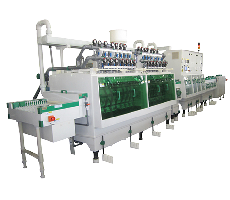
PCB加工中的蚀刻工艺

Jun. 09, 2022   |   1651 views

The process of printed circuit board from optical board to showing circuit pattern is a complex physical and chemical reaction process. This paper analyzes the last step - etching. At present, the typical process of printed circuit board (PCB) processing is "graphic electroplating". That is, a layer of lead tin anti-corrosion layer is pre plated on the copper foil to be retained on the outer layer of the board, that is, the graphic part of the circuit, and then the rest of the copper foil is chemically corroded, which is called etching.

蚀刻类型:

需要注意的是,蚀刻时板上有两层铜。在外层蚀刻过程中,只需要完全蚀刻一层铜,其余的将形成最终所需的电路。这种图案镀层的特征在于,镀铜层仅存在于铅锡耐腐蚀层下方。

Another process is that the whole board is plated with copper, and the parts other than the photosensitive film are only tin or lead tin corrosion resistant layers. This process is called "full plate copper plating process". Compared with pattern plating, the biggest disadvantage of copper plating on the whole board is that copper must be plated twice everywhere on the board, and they must be corroded during etching. Therefore, when the wire width is very fine, a series of problems will occur. At the same time, side corrosion will seriously affect the uniformity of lines.

在印刷电路板外电路的加工技术中,另一种方法是使用感光膜代替金属涂层作为防腐层。这种方法与内层蚀刻工艺非常相似。您可以参考内层制造过程中的蚀刻。

目前,锡或铅锡是最常用的抗蚀剂层,用于氨蚀刻剂蚀刻工艺。氨蚀刻剂是一种广泛使用的化学溶液,与锡或铅锡没有化学反应。氨蚀刻剂主要是指氨水/氯化铵蚀刻液。

此外,氨水/硫酸铵蚀刻溶液可以在市场上购买。硫酸盐基蚀刻溶液中的铜在使用后可以通过电解分离,因此可以重复使用。由于其腐蚀速率低,在实际生产中很少见到,但有望用于无氯蚀刻。

有人试图使用硫酸过氧化氢作为蚀刻剂来蚀刻外部图案。由于经济和废液处理等诸多原因,该工艺尚未在商业意义上得到广泛应用。此外,硫酸过氧化氢不能用于蚀刻铅锡抗蚀层,而且该工艺不是生产PCB外层的主要方法,因此大多数人很少关注它