
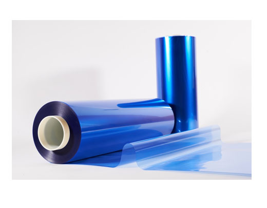
Function of PCB dry film
Dry film is a polymer compound. It can produce a polymerization reaction (the reaction process of synthesizing polymer from monomer) after ultraviolet irradiation to form a stable substance attached to the plate surface, so as to achieve the function of blocking electroplating and etching.
Dry film can be divided into four categories according to the thickness: (0.8mil, 1.2mil, 1.5mil, 2.0mil)
0.8mil thick dry film is mainly used for FPC fine circuit fabrication.
1.2mil dry film is mainly used for inner plate operation.
1.5mil dry film is mainly used for the operation of outer plate and of course it can also be used for the operation of inner plate. However, due to its thick thickness, it is easy to cause side corrosion in the etching process, and the cost is relatively high, so it is generally not used as the inner layer.
2.0mil dry film is mainly used for some plates with special requirements, such as large secondary holes. It can only be used when 1.5mil dry film cannot meet the requirements.
Structure of PCB dry film
It is generally divided into three layers, one is PE protective film, the middle is dry film layer, and the other is PET protective layer.PE layer and PET layer are only protective layers. They must be removed before film pressing and development. What really works is the middle layer of dry film, which has certain and good photosensitivity.
Main characteristics of PCB dry film
(1)Under the action of certain temperature and pressure, it will be firmly attached to the plate surface;
(2)Under certain light energy irradiation, it will absorb energy and cross-linking reaction will occur;The part not irradiated by light has no cross-linking reaction and can be dissolved by weak alkali solution.
PCB dry film storage environment
Constant temperature, constant humidity, yellow light, safe area.
Prevent storage with chemicals and radioactive substances.
In addition, the common quality defects of dry film include residual glue, exposure of foreign matters, poor vacuum pumping, unclean development, excessive development, open circuit, short circuit, line bulge, notch, exposed copper, film falling, line sawtooth, etc.
Common problems in dry film process
1) Residual film remains on the copper surface after development (unclean development).
2) The effect of mask method is poor.
3) The photoresist layer in the thinned conductor or unexposed area is not easy to be washed off during development (poor exposure).
4) The dry film is damaged during development or the dry film is warped or the edge is irregular after development (excessive development).
5) When the conductor is electroplated with tin and lead, the edge of the photoresist film is warped, resulting in tin infiltration (infiltration plating).
6) Dry film wrinkling.
7) Bubbles appear between the dry film and the copper surface of the substrate.

 May. 18, 2021


