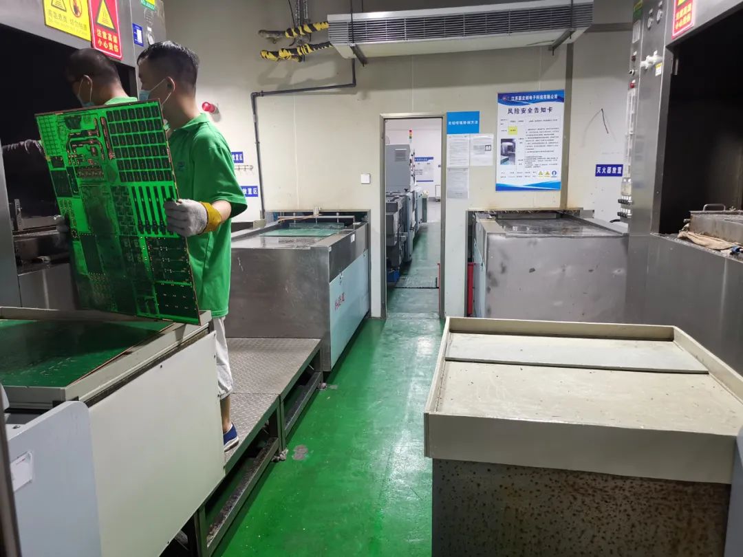
The current domestic PCB surface treatment processes include: spray tin (Hot Air Solder Leveling, HASL hot air leveling), OSP (anti-oxidation), full-board nickel-gold plating, immersion gold, immersion tin, immersion silver, chemical nickel-palladium-gold, electroplating For hard gold, there are some special PCB surface treatment processes for some special applications. A brief introduction is given below.
(1) Hot air leveling (tin spraying)
Hot air leveling is also known as hot air solder leveling (commonly known as tin spraying). It is a process of coating molten tin (lead) solder on the surface of the PCB and flattening (blowing) it with heated compressed air to form a layer that is both resistant to copper oxidation and can Provides a coating with good solderability. During hot air leveling, the solder and copper form a copper-tin intermetallic compound at the joint. When the PCB is leveled with hot air, it must be submerged in the molten solder. The air knife blows the liquid solder before the solder solidifies. The air knife can minimize the meniscus of the solder on the copper surface and prevent the solder from bridging. There are two types of hot air leveling: vertical and horizontal. It is generally considered that the horizontal type is better, and its coating is relatively uniform, and it is easy to realize automatic production.
① The advantages of HASL process are: low price and good welding performance.
② The disadvantage of the HASL process is that it is not suitable for welding pins with fine gaps and components that are too small, because the surface flatness of the tin spray board is poor, and it is easy to produce solder beads in the subsequent assembly process. It is easier to cause short circuits for fine pitch components.

(2) Organic solderability preservative (OSP) process
The organic solderability protective agent process is a process for the surface treatment of PCB copper foil that meets the requirements of the RoHS directive. Worldwide, 25%-30% of PCBs currently use OSP technology, and the proportion is still rising. The OSP process can be used on low-tech PCBs or high-tech PCBs, such as PCBs for single-sided TVs and PCBs for high-density chip packaging. For PCBs containing BGA devices, OSP applications are also more numerous. In fact, the OSP process will be the most ideal surface treatment process for applications where there are no functional requirements for surface connection or limited shelf life.
① The advantages of the OSP process are: the process is simple, the surface is very flat, suitable for lead-free soldering and SMT.
② The disadvantages of the OSP process are: nitrogen is required for soldering, and the number of reflow soldering is limited (multiple soldering will cause the film to be damaged, and there is no problem with the second time), it is not suitable for crimping technology, not suitable for rework and requires high storage conditions.
(3) The whole plate is plated with nickel and gold
Full-board nickel-plated gold is to plate a layer of nickel and then a layer of gold on the PCB surface conductor. The main purpose of nickel plating is to prevent the diffusion between gold and copper. At present, there are two main types of electroplated nickel gold: soft gold plating (pure gold, the surface does not look bright) and hard gold plating (the surface is smooth and hard, wear-resistant, contains other elements such as cobalt, and the surface looks brighter). Soft gold is mainly used for gold wire during chip packaging, and hard gold is mainly used for electrical interconnection in non-welded areas.
① The advantages of the gold-plating process are: longer storage time (>12 months), suitable for contact switch design and gold wire bonding, and suitable for electrical testing.
② The disadvantages of the gold plating process are: higher cost, thicker gold and poor consistency of the thickness of the gold layer. During the welding process, too thick gold may cause the solder joints to become brittle and affect the strength.
(4) Electroless nickel/immersion gold (ENIG)
Electroless nickel/immersion gold is also called immersion gold, which is a thick layer of nickel alloy with good electrical properties on the copper surface, which can protect the PCB for a long time. ENIG has environmental tolerance that other surface treatment processes do not have. In addition, immersion gold can also prevent the dissolution of copper, which will benefit lead-free assembly.
① The advantages of ENIG process are: it is not easy to oxidize, can be stored for a long time, and the surface is flat. It is suitable for soldering fine-gap pins and components with small solder joints. It can withstand multiple reflow soldering, is suitable for rework, and is suitable for use as COB. (Chip On Board) substrate for wire bonding.
② The disadvantages of ENIG process are: high cost, poor welding strength, easy to produce black disk problem, nickel layer will gradually oxidize over time, and long-term reliability is poor.

(5) Other surface treatment processes
Other surface treatment processes include immersion tin process, immersion silver process, chemical nickel palladium gold and electroplated hard gold.
① Immersion tin process: due to its good compatibility with solder, it has good solderability, and its flatness is excellent, suitable for lead-free soldering and crimping; the disadvantage is that it is not resistant to storage. It is best to have N2 protection during the welding process, and it is easy to produce “tin whiskers”.
② Immersion silver process: between organic coating and electroless nickel/immersion gold, the process is relatively simple, even if exposed to heat, humidity and polluted environment, silver can still maintain good solderability; the disadvantage is not It has the good physical strength of electroless nickel/immersion gold, high storage conditions, easy to contaminate, easy to oxidize, and at the same time, the welding strength is not good, and the problem of microvoids is easy to appear.
③ Chemical nickel-palladium-gold: Compared with immersion gold, there is an extra layer of palladium between nickel and gold, which has better corrosion resistance and strong resistance to environmental attacks. It is suitable for long-term storage and is suitable for lead-free soldering, thick plates and Switch contact design, etc.
④ Electroplating hard gold: often used in the “contact pair” of electrical connectors that require high wear resistance.

 Oct. 12, 2020