
1.总结
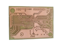
目前,印刷电路板(PCB)加工的典型工艺采用;图形电镀法”;也就是说,在铜箔上预镀一层铅锡耐腐蚀层,以保持在电路板的外层,即电路的图形部分,然后对铜箔的其余部分进行化学腐蚀,这被称为蚀刻。
需要注意的是,此时板上有两层铜。在外层蚀刻过程中,只需要完全蚀刻一层铜,其余的将形成最终所需的电路。这种图案镀的特征在于,镀铜层仅存在于铅锡抗蚀剂层下方。另一种工艺是在整个电路板上镀铜,除感光膜外的部分仅为锡或铅锡抗蚀层。此过程称为“;全板镀铜工艺”;与图案电镀相比,全板镀铜的最大缺点是必须在板表面各处镀两次铜,并且在蚀刻过程中必须被腐蚀。因此,当线宽非常细时,会出现一系列问题。同时,侧面腐蚀会严重影响线路的均匀性。
在印制板外电路的加工技术中,另一种方法是使用感光膜代替金属涂层作为防腐层。这种方法与内层蚀刻工艺非常相似。您可以参考内层制造过程中的蚀刻。
目前,锡或铅锡是最常用的抗蚀剂层,用于氨蚀刻剂的蚀刻过程。氨蚀刻剂是一种广泛使用的化学溶液,与锡或铅锡没有化学反应。氨蚀刻剂主要是指氨/氯化铵蚀刻溶液。此外,氨/硫酸铵蚀刻溶液也可以在市场上购买。
硫酸盐基蚀刻溶液中的铜在使用后可以通过电解分离,因此可以重复使用。由于其腐蚀速率低,在实际生产中通常很少见,但预计将用于无氯蚀刻。有人试图用硫酸过氧化氢作为蚀刻剂蚀刻外部图案。由于经济和废液处理等诸多原因,该工艺尚未在商业意义上得到广泛应用。此外,硫酸过氧化氢不能用于蚀刻铅锡抗蚀层,而且这一工艺不是PCB外层生产的主要方法,因此大多数人很少关注它。
2.蚀刻质量及存在的问题
蚀刻质量的基本要求是完全去除除抗蚀剂层下方之外的所有铜层,即;这就是全部。严格来说,如果要准确定义,蚀刻质量必须包括导体线宽的一致性和侧面腐蚀的程度。由于目前腐蚀性溶液的固有特性,它不仅可以向下蚀刻,还可以左右方向蚀刻,因此侧面腐蚀几乎是不可避免的。
蚀刻参数中经常讨论侧面蚀刻问题。它被定义为侧面蚀刻宽度与蚀刻深度的比值,称为蚀刻因子。在印刷电路行业,它从1:1到1:5变化很大。显然,小侧面蚀刻程度或低蚀刻因子是最令人满意的。
蚀刻设备的结构和不同成分的蚀刻溶液会影响蚀刻因子或侧面蚀刻程度,或者乐观地说,它是可以控制的。一些添加剂可以降低侧面腐蚀的程度。
在许多方面,蚀刻的质量早在印刷电路板进入蚀刻机之前就已经存在了。因为印刷电路加工的各种过程或过程之间存在着非常密切的内在联系,所以没有一个过程不受其他过程的影响,也不影响其他过程。许多被确定为蚀刻质量的问题实际上存在于之前的薄膜去除过程中,甚至更多。对于外部图形的蚀刻工艺,许多问题最终反映在它身上,因为其;逆流”;图像比大多数PCB工艺更突出。同时,这也是因为蚀刻是从薄膜粘贴和感光性开始的一系列工艺中的最后一步。之后,外部图案被成功转移。链接越多,出现问题的可能性就越大。这可以看作是印刷电路生产过程中一个非常特殊的方面。
从理论上讲,印刷电路进入蚀刻阶段后,在通过图形电镀加工印刷电路的过程中,理想的状态应该是电镀后铜和锡或铜和铅锡的总厚度不应超过耐电镀感光膜的厚度,这样电镀图案就完全被电镀图案阻挡;墙壁”;然而,在实际生产中,经过电镀后,世界各地印刷电路板的镀层图案都比感光图案厚得多。在电镀铜和铅锡的过程中,由于镀层高度超过感光膜,有横向积累的趋势,出现了问题。覆盖在条带上方的锡或铅锡抗蚀剂层延伸到两侧;边缘”;,并且感光膜的一小部分被覆盖在“;边缘”;。
“;边缘”;由锡或铅锡形成的薄膜使得在去除薄膜时无法完全去除感光薄膜;残留胶水”;在“;边缘”;. “残留胶水”;或者“;残留薄膜”;留在“;边缘”;抗蚀剂的剥离将导致蚀刻不完全。线条形成“;铜根”;在蚀刻后的两侧,线间距变窄,导致印刷板不符合甲方的要求,甚至可能被拒收。拒收将大大增加PCB的生产成本。
此外,在许多情况下,溶解是由于反应形成的。在印刷电路行业中,残留的薄膜和铜也可能积聚在腐蚀性溶液中,堵塞腐蚀性机器和耐酸泵的喷嘴,因此必须停机进行处理和清洗,这会影响工作效率。
3.设备调整及与腐蚀性溶液的相互作用
在印刷电路加工中,氨蚀刻是一个相对精细和复杂的化学反应过程。相反,这是一项容易的工作。一旦调整了工艺,就可以进行连续生产。关键是机器一旦启动,就需要保持连续的工作状态,不应该停止。蚀刻过程在很大程度上取决于设备的良好工作状态。目前,无论使用哪种蚀刻溶液,都必须使用高压喷涂,为了获得整齐的线条边和高质量的蚀刻效果,必须严格选择喷嘴结构和喷涂方式。
为了获得良好的副作用,出现了许多不同的理论,形成了不同的设计方法和设备结构。这些理论往往大相径庭。然而,所有关于蚀刻的理论都承认最基本的原则,即尽快使金属表面与新鲜的蚀刻溶液接触。蚀刻过程的化学机理分析也证实了上述观点。在氨蚀刻中,假设所有其他参数保持不变,蚀刻速率主要由蚀刻溶液中的氨(NH3)决定。因此,新溶液和蚀刻表面之间的相互作用有两个主要目的:一是冲洗掉新产生的铜离子;第二种是连续提供反应所需的氨(NH3)。
在印刷电路行业的传统知识中,特别是印刷电路原材料的供应商,人们认识到氨蚀刻溶液中单价铜离子的含量越低,反应速度就越快。经验已经证实了这一点。事实上,许多氨蚀刻剂产品含有单价铜离子的特殊配位基团(一些复杂的溶剂),用于还原单价铜离子(这些是其产品具有高反应能力的技术秘密)。可以看出,单价铜离子的影响不小。如果单价铜从5000ppm减少到50ppm,蚀刻速率将增加一倍以上。
由于蚀刻反应过程中会产生大量的一价铜离子,并且由于一价铜离子总是与氨的络合物紧密结合,因此很难将其含量保持在接近零的水平。通过大气中的氧气作用,将单价铜转化为二价铜,可以去除单价铜。上述目的可以通过喷涂来实现。
这是将空气通入蚀刻箱的功能原因。但是,如果空气太多,会加速溶液中氨的损失,降低pH值,这仍然会降低蚀刻速率。溶液中的氨也需要控制。一些用户使用将纯氨通入蚀刻储罐的方法。为此,必须添加一套pH计控制系统。当自动测量的pH值低于给定值时,溶液将自动添加。
在化学蚀刻(也称为光化学蚀刻或PCH)的相关领域,研究工作已经开始,并已达到蚀刻机结构设计阶段。在这种方法中,使用的溶液是二价铜,而不是氨铜蚀刻。它很可能会用于印刷电路行业。在PCH行业,蚀刻铜箔的典型厚度为5至10密耳,在某些情况下甚至相当大。它对蚀刻参数的要求往往比PCB行业更严格。PCM工业系统的一项研究成果尚未正式发表,但结果将令人耳目一新。在强大的项目资金支持下,研究人员有能力从长远意义上改变蚀刻装置的设计理念,并研究这些变化的影响。例如,与锥形喷嘴相比,最佳的喷嘴设计采用扇形,喷雾收集室(即喷嘴拧入的管道)也有一个安装角度,可以将进入蚀刻室的工件以30度的角度喷雾。如果不进行这样的更改,收集器上喷嘴的安装方式将导致每个相邻喷嘴的喷射角度不一致。第二组喷嘴的喷雾表面与第一组略有不同(这表明喷雾的工作状态)。这样,喷雾溶液的形状变成叠加或交叉状态。从理论上讲,如果溶液形状相互交叉,这部分的喷射力会降低,蚀刻表面上的旧溶液不能被有效地冲走,使新溶液与之接触。这种情况在喷射表面的边缘尤为突出。其喷射力远小于垂直方向上的喷射力。
研究发现,最新的设计参数为65磅/平方英寸(即4巴)。每种蚀刻工艺和每种实用解决方案都有一个最佳的注入压力。目前,蚀刻室中的注射压力超过30磅/平方英寸(2bar)。蚀刻溶液的密度(即比重或波美度)越高,最佳注入压力就越高。当然,这不是一个单一的参数。另一个重要参数是溶液中反应速率的相对迁移率。
4.在上下板表面,前缘和后缘的蚀刻状态不同。
与蚀刻质量相关的大量问题集中在上板表面的蚀刻部分。理解这一点很重要。这些问题源于蚀刻剂在印刷电路板上表面产生的胶体结构的影响。铜表面的胶体沉积物一方面影响喷射力,另一方面阻碍新鲜蚀刻溶液的补充,导致蚀刻速度降低。正是由于胶体结构的形成和积累,电路板上下图形的蚀刻程度不同。这也使得蚀刻机中的板的第一部分容易被彻底蚀刻或容易引起过度腐蚀,因为当时没有形成积聚,蚀刻速度很快。相反,当板后面的部分进入时,堆积物已经形成,其蚀刻速度减慢。
5.蚀刻设备的维护
维护蚀刻设备的关键因素是确保喷嘴清洁、畅通无阻。堵塞或结渣会在喷射压力的作用下影响布局。如果喷嘴变脏,会导致蚀刻不均匀,并报废整个PCB。
显然,设备的维护是更换损坏和磨损的零件,包括喷嘴。喷嘴也有磨损的问题。此外,更关键的问题是保持蚀刻机没有结渣,这在许多情况下都会发生。过多的结渣堆积甚至会影响蚀刻溶液的化学平衡。同样,如果蚀刻溶液中存在过度的化学不平衡,结渣将变得越来越严重。结渣和堆积的问题怎么强调都不为过。一旦蚀刻溶液中突然出现大量结渣,通常是溶液平衡错误的信号。这应该用浓盐酸适当清洗或添加到溶液中。
残留的薄膜也会产生熔渣。极少量的残留膜溶解在蚀刻溶液中,然后形成铜盐沉淀。残余薄膜形成的结渣表明之前的薄膜去除过程没有完成。薄膜去除不良通常是边缘薄膜和过度镀层的结果。

 2019年12月20日


