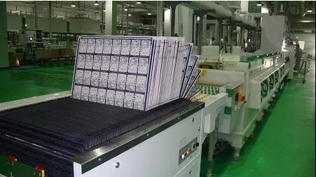
PCB板外电路的蚀刻工艺

Oct. 29, 2021   |   1784 views

1、PCB板外电路的蚀刻工艺

At present, the typical process of printed circuit board (PCB) processing adopts "Pattern electroplating method". A layer of lead tin corrosion resistant layer is pre plated on the copper foil to be retained on the outer layer of the board, the pattern part of the circuit, and then the rest of the copper foil is chemically corroded, which is called etching. 


It should be noted that there are two layers of copper on the board at this time. In the outer etching process, only one layer of copper must be completely etched, and the rest will form the final required circuit.This type of pattern plating is characterized in that the copper plating layer only exists below the lead tin resist layer.Another process is that the whole board is plated with copper, and the part other than the photosensitive film is only tin or lead tin resist layer.This process is called "full plate copper plating process".Compared with pattern plating, the biggest disadvantage of full board copper plating is that copper must be plated twice everywhere on the board, and they must be corroded during etching.Therefore, when the wire width is very fine, a series of problems will arise.At the same time, side corrosion will seriously affect the uniformity of lines.

在印制板外电路的加工技术中,另一种方法是使用感光膜代替金属涂层作为防腐层。这种方法与内层蚀刻工艺非常相似。您可以参考内层制造过程中的蚀刻。

目前,锡或铅锡是最常用的抗蚀剂层,用于氨蚀刻剂的蚀刻过程。氨蚀刻剂是一种广泛使用的化学溶液,它与锡或铅锡没有化学反应。氨蚀刻剂主要是指氨/氯化铵蚀刻溶液。此外,氨/硫酸铵蚀刻溶液也可以在市场上购买。

硫酸盐基蚀刻溶液中的铜在使用后可以通过电解分离,因此可以重复使用。干法蚀刻的腐蚀速率较低,在实际生产中通常很少见,但预计将用于无氯蚀刻。有人试图用硫酸过氧化氢作为蚀刻剂蚀刻外部图案。由于经济和废液处理等诸多原因,该工艺尚未在商业意义上得到广泛应用。此外,硫酸过氧化氢不能用于蚀刻铅锡抗蚀层,而且这一工艺不是PCB外层生产的主要方法,因此大多数人很少关注它。

2、蚀刻质量及存在的问题

The basic requirement for etching quality is to completely remove all copper layers except under the resist layer, that's all.Strictly speaking, if it is to be accurately defined, the etching quality must include the consistency of conductor linewidth and the degree of side corrosion.Due to the inherent characteristics of the current corrosive solution, it can etch not only downward, but also left and right directions, so side corrosion is almost inevitable.

蚀刻参数中经常讨论侧面蚀刻问题。它被定义为侧面蚀刻宽度与蚀刻深度的比值,称为蚀刻因子。在印刷电路行业,它从1:1到1:5变化很大。显然,小侧面蚀刻程度或低蚀刻系数是最令人满意的。

蚀刻设备的结构和不同成分的蚀刻溶液会影响蚀刻因子或侧面蚀刻程度,或者乐观地说,它是可以控制的。一些添加剂可以降低侧面腐蚀的程度。这些添加剂的化学成分通常是商业机密,其开发者不会向外界披露。关于蚀刻设备的结构,以下章节将进行讨论。

In many ways, the quality of etching has existed long before the printed board entered the etching machine.Because there is a very close internal relationship between various processes or processes of printed circuit processing, there is no process that is not affected by other processes and does not affect other processes.Many problems identified as etching quality have actually existed in the previous process of film removal or even more.For the etching process of outer graphics, many problems are finally reflected in it because its "inverted stream" image is more prominent than most PCB processes.At the same time, this is also because etching is the last step in a long series of processes starting from film pasting and photosensitivity. After that, the outer pattern is transferred successfully.The more links, the greater the possibility of problems.This can be regarded as a very special aspect in the production process of printed circuit. 

Theoretically, after the printed circuit enters the etching stage, in the process of processing printed circuit by pattern electroplating, the ideal state should be: the total thickness of copper and tin or copper and lead tin after electroplating should not exceed the thickness of electroplating resistant photosensitive film, so that the electroplating pattern is completely blocked by the "wall" on both sides of the film and embedded in it.However, in real production, after electroplating, the plated graphics of printed circuit boards all over the world should be greatly thick and dry.In the process of electroplating copper and lead tin, because the coating height exceeds the photosensitive film, there is a trend of transverse accumulation, and the problem arises.The tin or lead tin resist layer covered above the strip extends to both sides to form a "edge", and a small part of the photosensitive film is covered under the "edge". 

The "edge" formed by tin or lead tin makes it impossible to completely remove the photosensitive film when removing the film, leaving a small part of the "residual glue" under the "edge".If the "residual glue" or "residual film" is left under the "edge" of the resist, it will cause incomplete etching. After etching, a "copper root" is formed on both sides of the line, which narrows the line spacing, resulting in the printed board not meeting the requirements of Party A and may even be rejected. Due to rejection, the production cost of PCB will be greatly increased. 

此外,在许多情况下,溶解是由于反应形成的。在印刷电路行业中,残留的薄膜和铜也可能积聚在腐蚀性溶液中,堵塞腐蚀性机器和耐酸泵的喷嘴,因此必须停机进行处理和清洗,这会影响工作效率。 

3、设备调整及与腐蚀性溶液的相互作用

在印刷电路加工中,氨蚀刻是一个相对精细和复杂的化学反应过程。另一方面,这是一项容易的工作。一旦调整了工艺,就可以连续生产。关键是机器启动后要保持连续工作状态,不宜干燥或停止。蚀刻过程在很大程度上取决于设备的良好工作状态。例如,无论使用哪种蚀刻溶液,都必须使用高压喷涂。为了获得整齐的线条边和高质量的蚀刻效果,必须严格选择喷嘴的结构和喷涂方式。

为了获得良好的副作用,出现了许多不同的理论,形成了不同的设计方法和设备结构。这些理论往往大相径庭。然而,所有与蚀刻相关的理论都认识到最基本的原则,即尽快使金属表面与新鲜的蚀刻溶液接触。蚀刻过程的化学机理分析也证实了在氨蚀刻中,假设所有其他参数保持不变,蚀刻速率主要由蚀刻溶液中的氨(NH3)决定。因此,使用新鲜溶液与蚀刻表面相互作用有两个主要目的:一是冲洗掉新产生的铜离子;另一种是连续提供反应所需的氨(NH3)。

在印刷电路行业的传统知识中,特别是印刷电路原材料的供应商,人们认识到氨蚀刻溶液中单价铜离子的含量越低,反应速度就越快,这一点已被经验证实。事实上,许多氨蚀刻溶液产品都含有单价铜离子的特殊配位基团(一些复杂的溶剂),其功能是还原单价铜离子(这些都是其产品具有高反应能力的技术秘密)。可以看出,单价铜离子的影响不小。如果单价铜从5000ppm减少到50ppm,蚀刻速率将增加一倍以上。 

因为在蚀刻反应过程中会产生大量的一价铜离子,并且因为一价铜离子总是与氨的络合物紧密结合,所以很难将它们的含量保持在接近零的水平。通过大气中的氧气作用,将单价铜转化为二价铜,可以去除单价铜。上述目的可以通过喷涂来实现。