
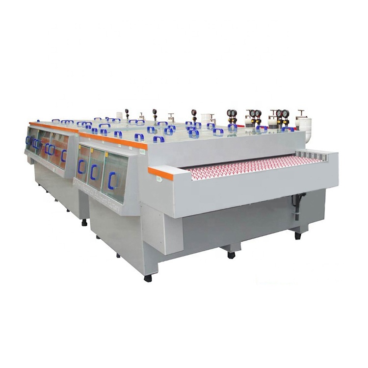
Der Prozess der Leiterplatte von der optischen Leiterplatte zur Anzeige des Schaltungsmusters ist ein relativ komplexer physikalischer und chemischer Reaktionsprozess. Dieses Papier analysiert den letzten Schritt – Ätzung. Derzeit ist der typische Prozess der Verarbeitung von Leiterplatten (PCB) “ Muster Beschichtung” Das heißt, eine Schicht aus Blei-Zinn-Korrosionsschutzschicht wird auf dem Kupferfolienteil vorbeschichtet, das auf der Außenschicht der Platte, d. h. dem grafischen Teil der Schaltung, gehalten werden soll, und dann wird der Rest der Kupferfolie chemisch korrodiert, was Ätzung genannt wird.
Art des Ätzens:
Es ist zu beachten, dass es beim Ätzen zwei Kupferschichten auf der Platte gibt. Im Ätzprozess der Außenschicht muss nur eine Kupferschicht vollständig geätzt werden, und der Rest bildet den endgültigen erforderlichen Kreislauf. Diese Art der Mustergegalvanisierung ist dadurch gekennzeichnet, dass die Kupferbeschichtungsschicht nur unterhalb der Blei-Zinn-korrosionsbeständigen Schicht besteht.
Ein weiterer Prozess besteht darin, dass die gesamte Platte mit Kupfer beschichtet ist, und der Teil außerhalb des lichtempfindlichen Films ist nur Zinn oder Blei Zinn korrosionsbeständige Schicht. Dieser Prozess heißt “ Vollplatz Kupferbeschichtungsprozess” Im Vergleich zur Musterbeschichtung besteht der größte Nachteil der Kupferbeschichtung auf der gesamten Platte darin, dass Kupfer zweimal überall auf der Platte beschichtet werden muss und sie beim Ätzen korrodiert werden müssen. Wenn die Drahtbreite sehr fein ist, treten daher eine Reihe von Problemen auf. Gleichzeitig wird die Seitenkorrosion die Gleichmäßigkeit der Linien ernsthaft beeinflussen.
In der Verarbeitungstechnik der äußeren Schaltung der Leiterplatte besteht ein anderes Verfahren, nämlich die Verwendung der lichtempfindlichen Folie anstelle der Metallbeschichtung als Korrosionsschutzschicht. Diese Methode ist dem Ätzprozess der Innenschicht sehr ähnlich, und Sie können sich auf das Ätzen im Herstellungsprozess der Innenschicht beziehen.
Derzeit ist Zinn oder Bleizinn die am häufigsten verwendete Resistschicht, die im Ätzprozess von Ammoniak-Ätzmittel verwendet wird. Ammoniak-Ätzmittel ist eine weit verbreitete chemische Lösung, die keine chemische Reaktion mit Zinn oder Bleizinn hat. Ammoniak Ätzmittel bezieht sich hauptsächlich auf Ammoniakwasser / Ammoniakchlorid Ätzlösung.
Darüber hinaus kann auf dem Markt auch Ammoniakwasser / Ammoniaksulfat Ätzlösung gekauft werden. Das Kupfer in sulfatbasierter Gravierlösung kann nach dem Gebrauch durch Elektrolyse getrennt werden, so dass es wiederverwendet werden kann. Aufgrund seiner niedrigen Korrosionsrate ist es in der Regel selten in der tatsächlichen Produktion, aber es wird erwartet, dass es im chlorfreien Ätzen verwendet wird.
Jemand versuchte, Schwefelsäurewasserstoffperoxid als Ätzmittel zu verwenden, um das äußere Muster zu Ätzen. Aus vielen Gründen, einschließlich Wirtschaft und Abfallflüssigkeitsbehandlung, wurde dieser Prozess im kommerziellen Sinne nicht weit verbreitet Darüber hinaus kann Schwefelsäurewasserstoffperoxid nicht für das Ätzen von Blei-Zinn-Resistschicht verwendet werden, und dieser Prozess ist nicht die Hauptmethode bei der Herstellung von PCB-Außenschicht, so dass die meisten Menschen selten darauf achten.
Ätzqualität und bereits bestehende Probleme:
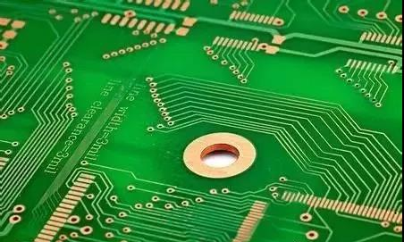
Die Grundvoraussetzung für Ätzqualität besteht darin, alle Kupferschichten außer unter der Korrosionsschutzschicht vollständig zu entfernen, und das’ S alle. Streng gesagt, wenn wir es genau definieren wollen, muss die Ätzqualität die Konsistenz der Drahtbreite und den Grad der Seitenerosion umfassen. Aufgrund der inhärenten Eigenschaften der aktuellen korrosiven Lösung kann sie nicht nur nach unten, sondern auch links und rechts Ätzen, so dass Seitenerosion fast unvermeidlich ist.
Das seitliche Ätzproblem wird in den Ätzparametern häufig diskutiert. Es wird definiert als das Verhältnis der SeitenÄtzbreite zur Ätztiefe, das als Ätzfaktor bezeichnet wird. In der Leiterplattenindustrie gibt es eine breite Palette von Veränderungen, von 1:1 bis 1:5. Natürlich ist ein kleiner Seitenätz oder ein niedriger Ätzfaktor der zufriedenstellendste.
Die Struktur der Ätzgeräte und die Ätzlösung mit unterschiedlichen Komponenten wird sich auf den Ätzfaktor oder den SeitenÄtzgrad auswirken, oder in einem optimistischen Wort, sie kann gesteuert werden. Der Seitenkorrosionsgrad kann durch den Einsatz einiger Zusatzstoffe reduziert werden. Die chemischen Komponenten dieser Zusatzstoffe sind in der Regel Geschäftsgeheimnisse und ihre jeweiligen Entwickler geben sie der Außenwelt nicht offen.
In vielerlei Hinsicht hat die Qualität des Ätzens lange existiert, bevor gedruckte Platten in die Ätzmaschine gelangen. Da es eine sehr enge interne Verbindung zwischen den verschiedenen Prozessen oder Prozessen der Druckkreisverarbeitung gibt, gibt es keinen Prozess, der nicht von anderen Prozessen beeinflusst wird und andere Prozesse nicht beeinflusst. Viele Probleme, die als Ätzqualität identifiziert wurden, existierten bereits im früheren Prozess der Filmentfernung oder sogar mehr.
Für den Ätzprozess von äußeren Grafiken spiegeln sich schließlich viele Probleme darin wider, weil seine “ Umkehrter Strom” Bild ist prominenter als die meisten PCB-Prozesse. Gleichzeitig liegt dies auch daran, dass Ätzen der letzte Schritt in einer langen Reihe von Prozessen ist, beginnend mit der Selbstbeschichtung und der Lichtempfindlichkeit. Danach wird das äußere Muster erfolgreich übertragen. Je mehr Links, desto größer ist die Möglichkeit von Problemen. Dies kann als sehr besonderer Aspekt im Produktionsprozess der Leiterplatte angesehen werden.
Theoretisch gesehen sollte, nachdem die gedruckte Schaltung in die Ätzstufe eintritt, bei der Verarbeitung der gedruckten Schaltung durch Mustergegalvanisierung der ideale Zustand sein: die Gesamtdicke von Kupfer und Zinn oder Kupfer und Blei Zinn nach der Galvanisierung sollte die Dicke des Galvanisierungsbeständigen lichtempfindlichen Films nicht überschreiten, so dass das Galvanisierungsmuster vollständig von der “ Wände” auf beiden Seiten der Folie und in sie eingebettet. In der realen Produktion ist jedoch das plattierte Muster von Leiterplatten auf der ganzen Welt viel dicker als das lichtempfindliche Muster nach der Galvanisierung. Bei der Galvanisierung von Kupfer und Blei Zinn, da die Beschichtungshöhe den lichtempfindlichen Film übersteigt, gibt es einen Trend der horizontalen Ansammlung, die zu Problemen führt. Die Zinn- oder Blei-Zinn-Korrosionsschutzschicht, die über der Linie bedeckt ist, erstreckt sich auf beiden Seiten, um eine “ Rand” bedeckt einen kleinen Teil des lichtempfindlichen Films unter dem “ edge”.
Die “ Rand” gebildet durch Zinn oder Blei Zinn macht es unmöglich, den lichtempfindlichen Film bei der Entfernung des Films vollständig zu entfernen, wobei ein kleiner Teil des “ Restkleber” unter dem “ Rand” . “ Restkleber” oder “ mein Film” links unter dem “ Rand” des Widerstands wird unvollständige Ätzung verursachen. Die Linien bilden “ Kupferwurzeln” auf beiden Seiten nach dem Ätzen, was den Linienabstand verkürzt, was dazu führt, dass die gedruckte Platte Partei A nicht erfüllt; Anforderungen und können sogar abgelehnt werden. Ablehnung wird die Produktionskosten von PCB erheblich erhöhen.
Darüber hinaus entsteht in vielen Fällen aufgrund der Reaktion eine Lösung. In der Leiterplattenindustrie können sich Restfilm und Kupfer auch in der korrosiven Lösung ansammeln und in der Düse der korrosiven Maschine und der säurebeständigen Pumpe blockieren, so dass sie zur Behandlung und Reinigung geschlossen werden müssen, was die Arbeitseffizienz beeinflusst.

 9. November 2021


